Repair K.M.E. SPA500F power amplifier

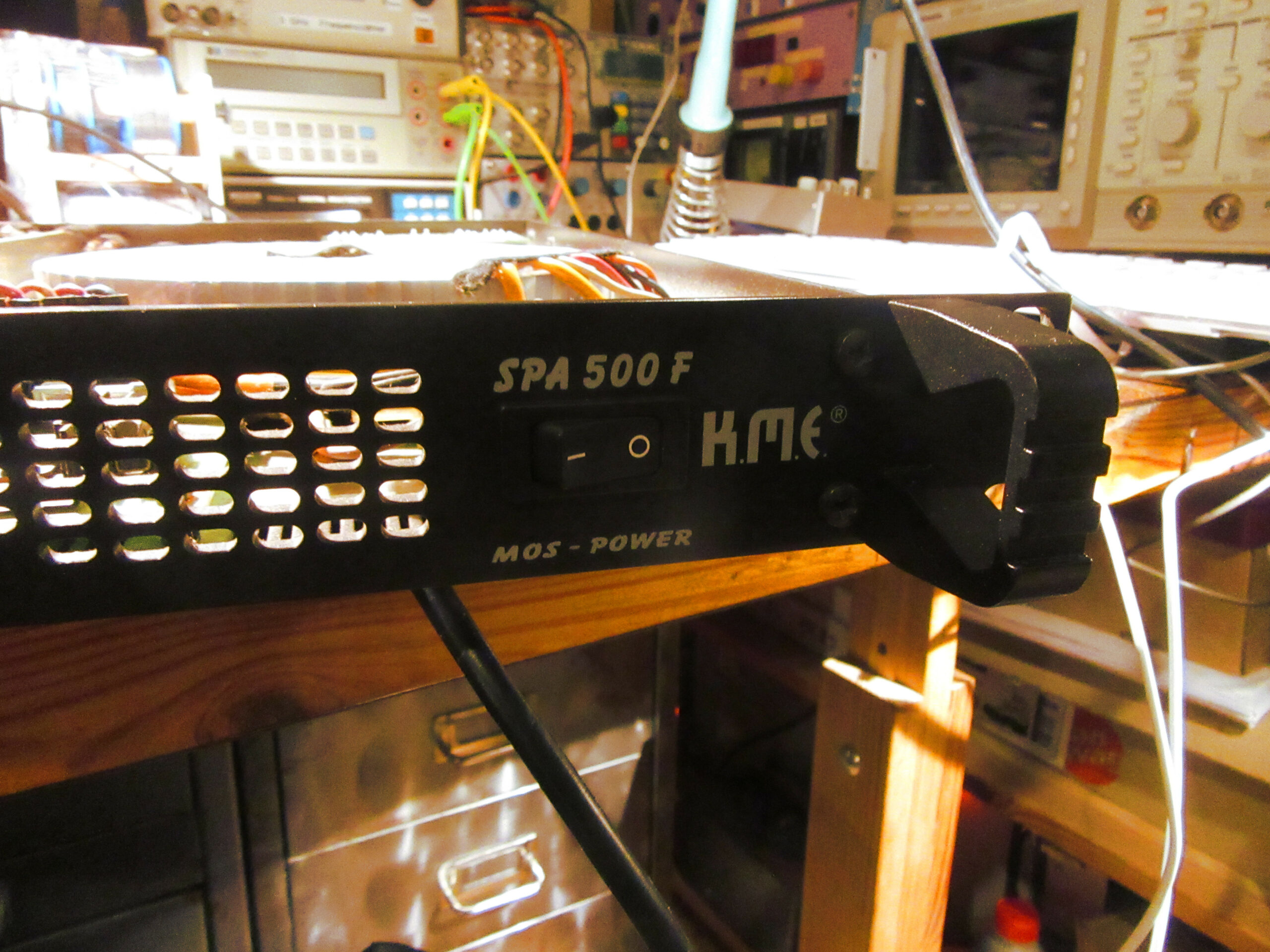
My friend Falk asked me at the beginning of the year if I would take a look at a defective power amplifier that he could buy very cheaply on the Internet. In my opinion, you could not go wrong with it, since the built-in power transformer alone was worth the purchase price. So the power amplifier was ordered and immediately delivered to my home. It was a device from the company K.M.E., model SPA500F with 2x 250W RMS into 4 ohms or 2x 150W RMS into 8 ohms. The year of manufacture was about 2000.The seller described the condition something like this: “One channel does not work, the rest is in top condition, also do not know.” After two days of shipping, the part was with me. The rest of the story I tell as a small picture story below.

Inventory

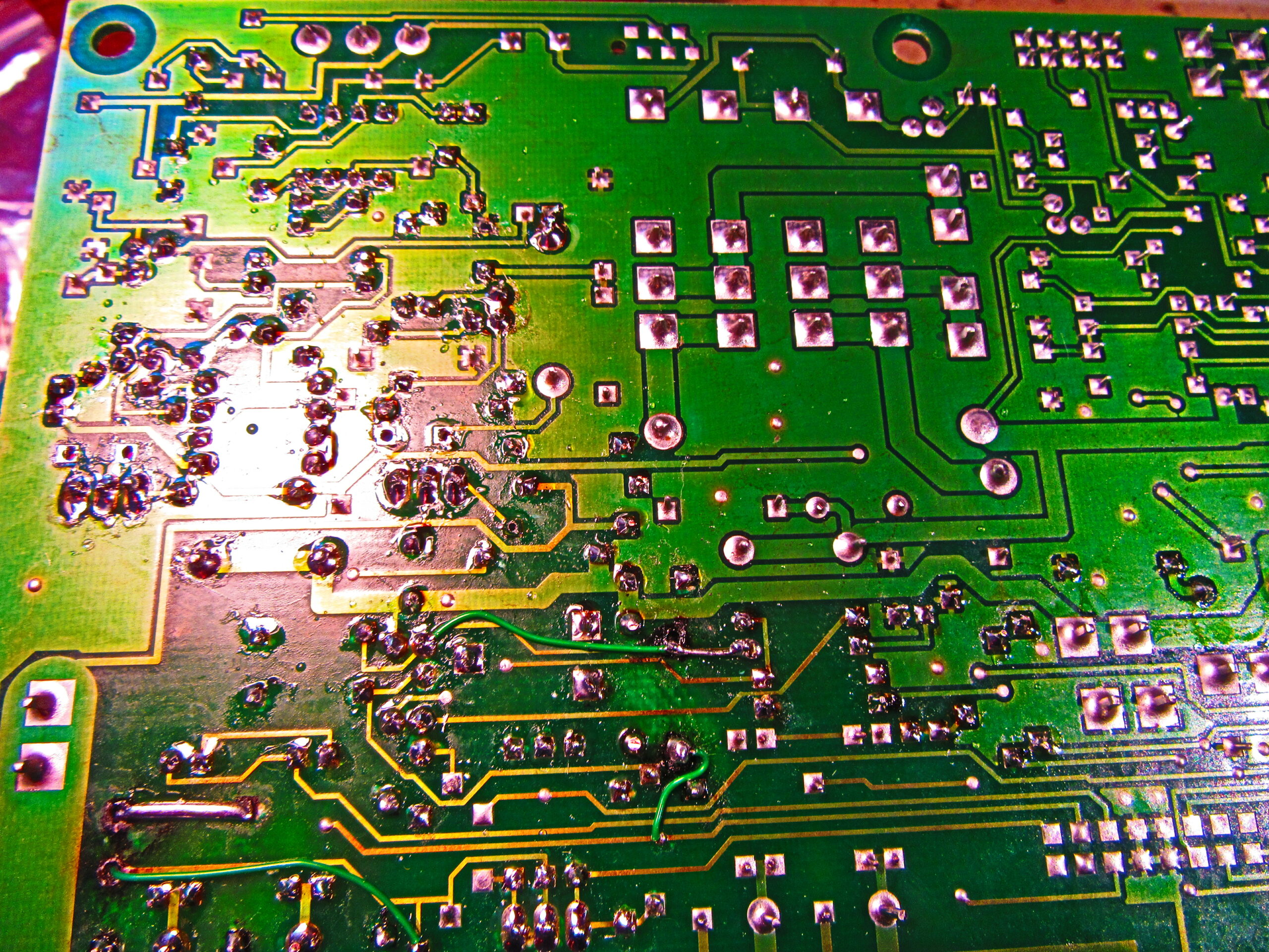
The first thing to do was the initial inspection, i.e. unscrew the casing cover and take a look.

Housing opened on the workbench

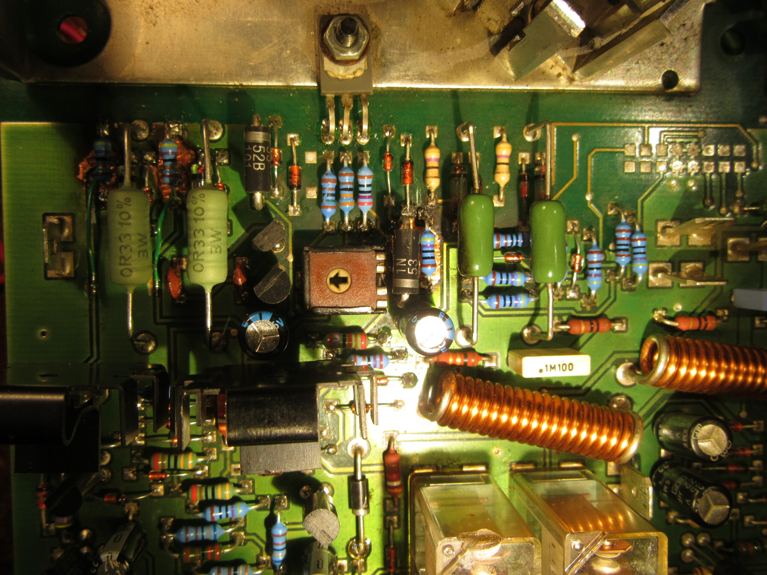
A strong smell of cold cigarette smoke and burnt electronics and corresponding deposits gave away: The device had been used for years in an environment with a lot of nicotine, probably a discotheque.

Brown deposits on the heat sink

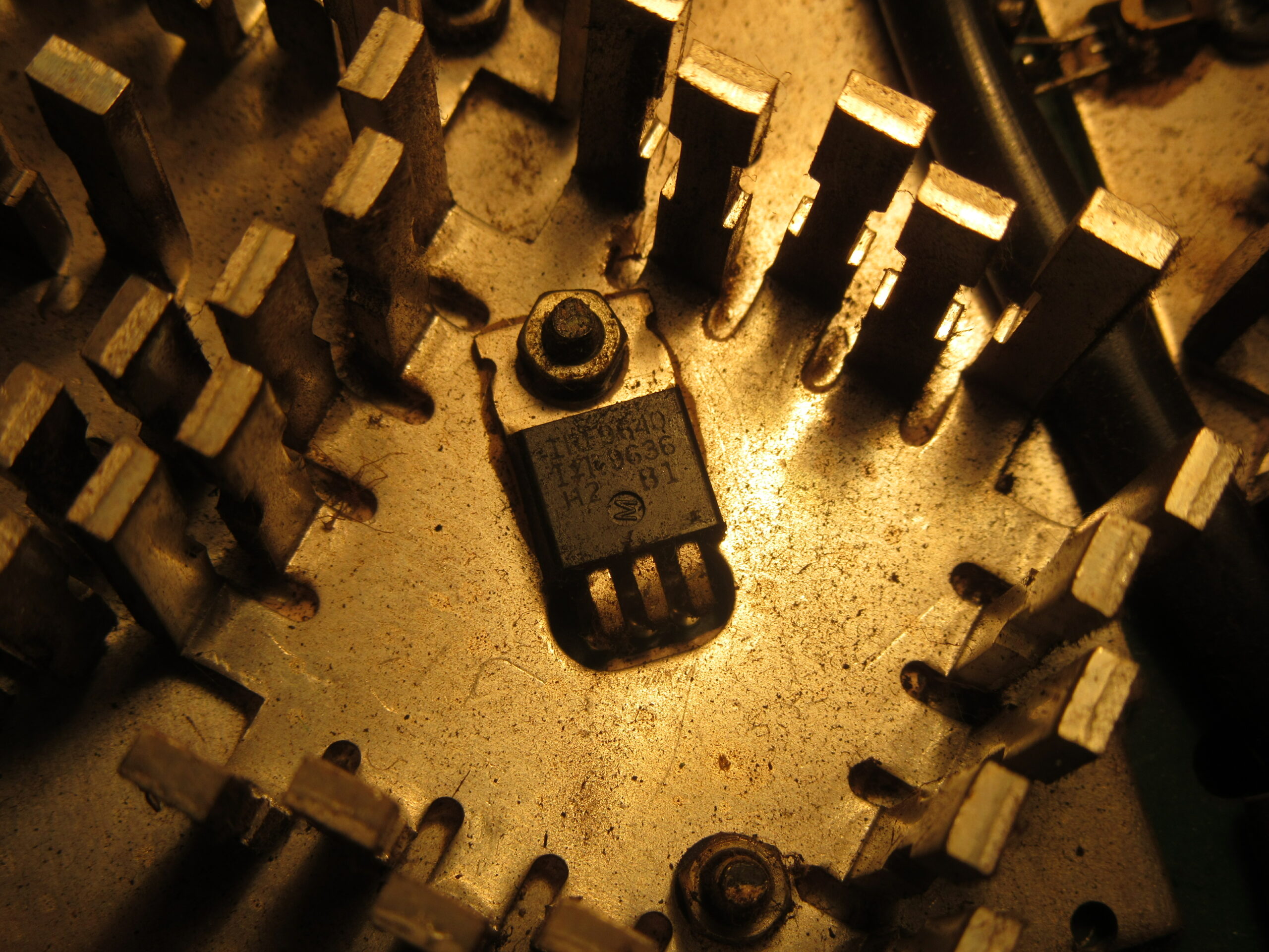
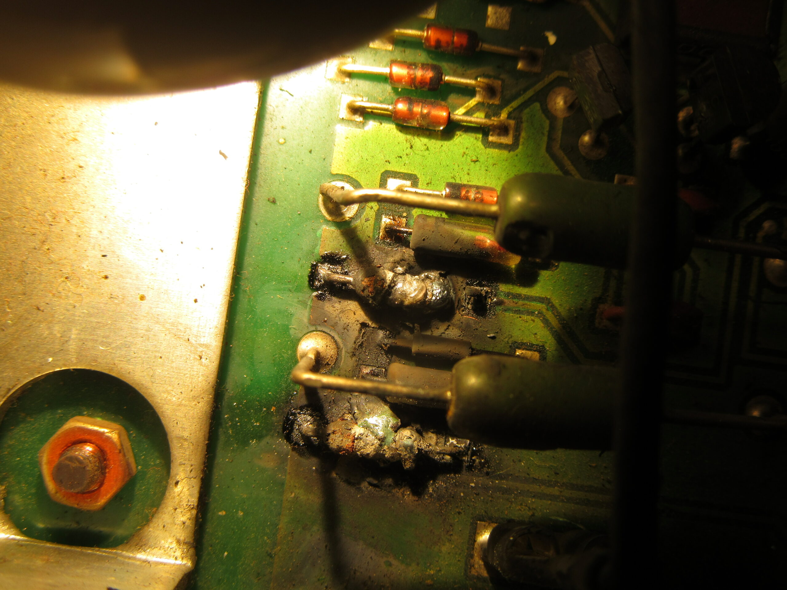
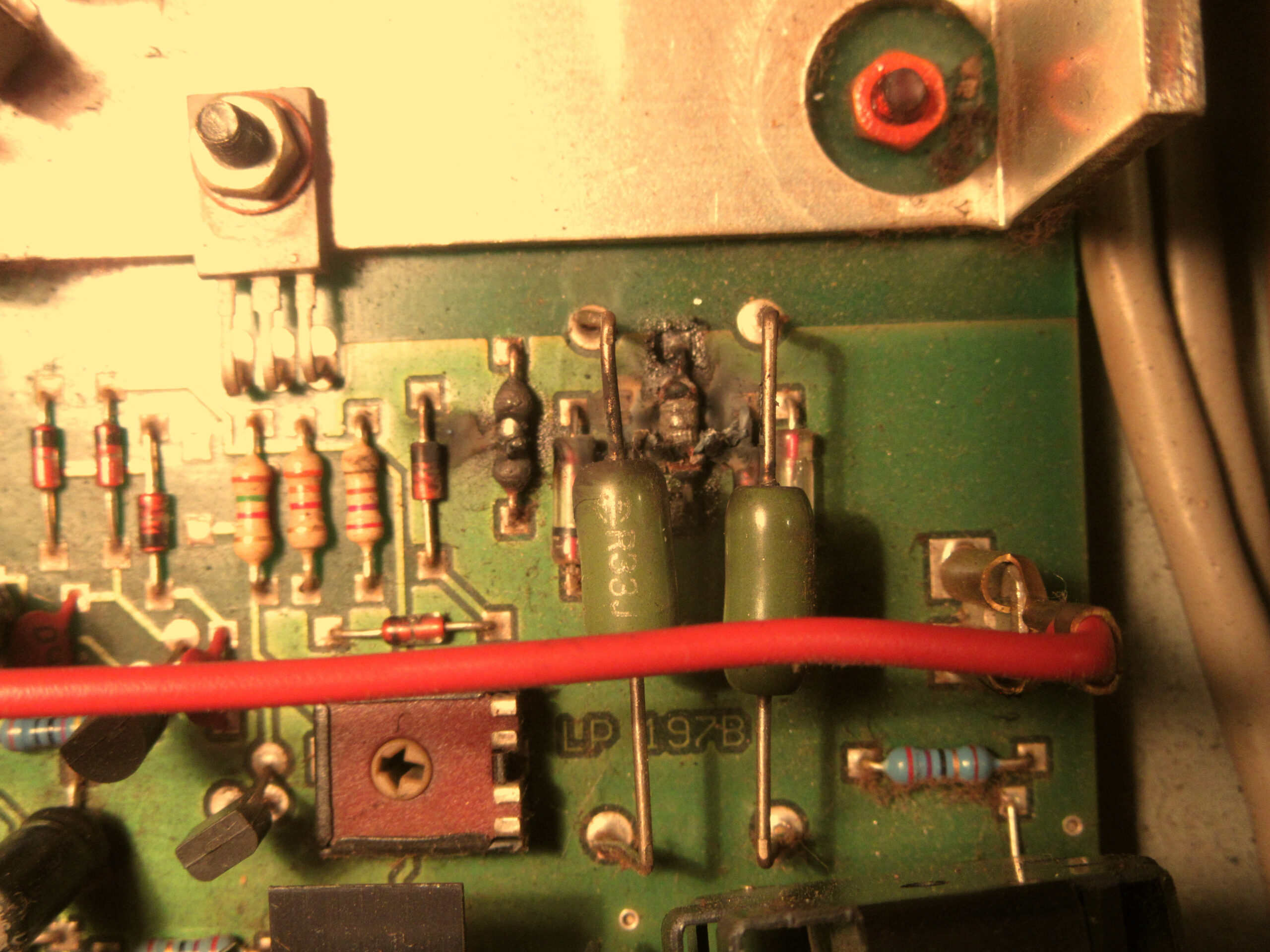
In addition, a lot of components on the board had burned or even exploded.

Burn marks in the housing cover

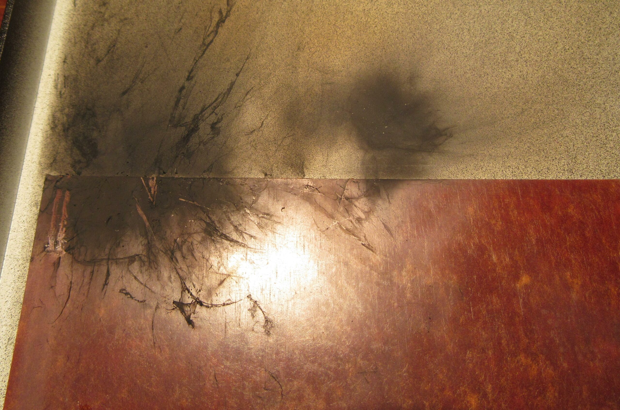
It was also clear that the unit had recently been opened. With the burn marks on the lid and the smell, both of which are hard to miss, the seller may not have been completely honest in his condition description.

Here are some pictures of the exciting parts.

Gate resistors of the output transistors
Gate resistors from positive branch
More burned out parts
A picture of devastation

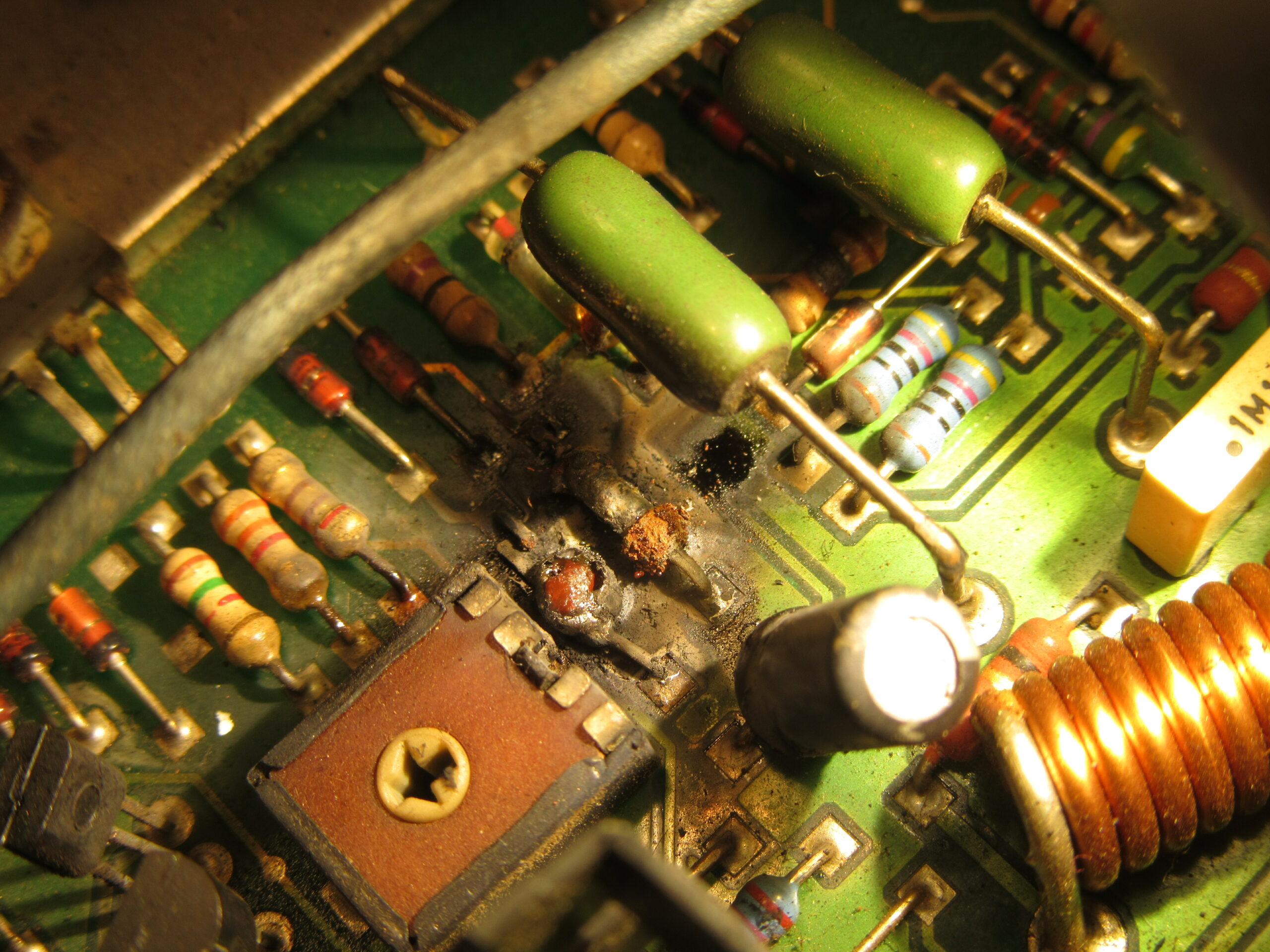
Also some traces had dissolved into nothing. It quickly became clear that I would not get anywhere here without a circuit diagram. A search for the documents on the Internet yielded nothing, so without further ado I sent a friendly request to the service email of K.M.E. over the weekend. And voila, on Monday morning, the schematic and assembly diagram were in my inbox, sent by the production manager himself. Many thanks again at this point.
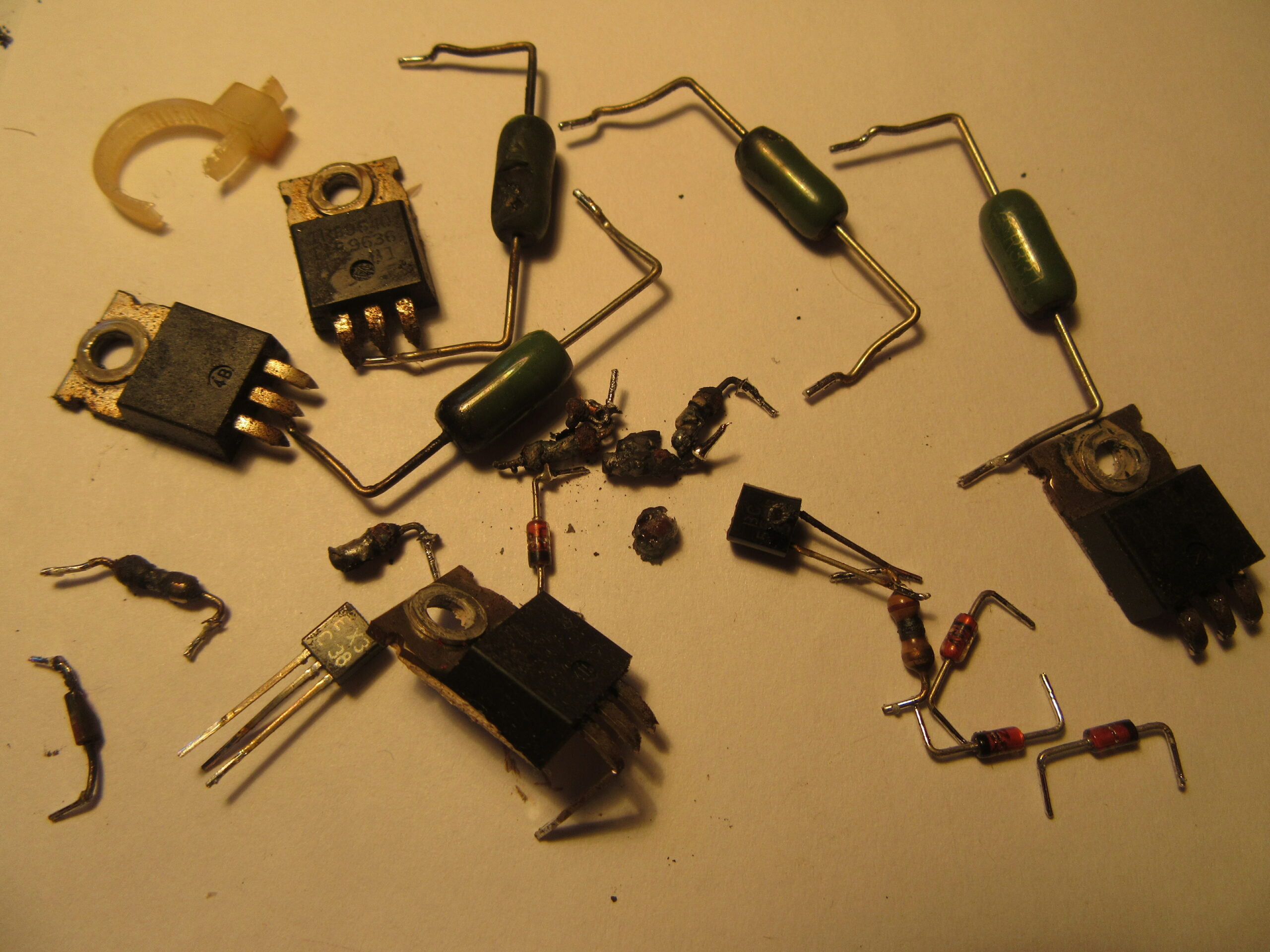
Defective parts

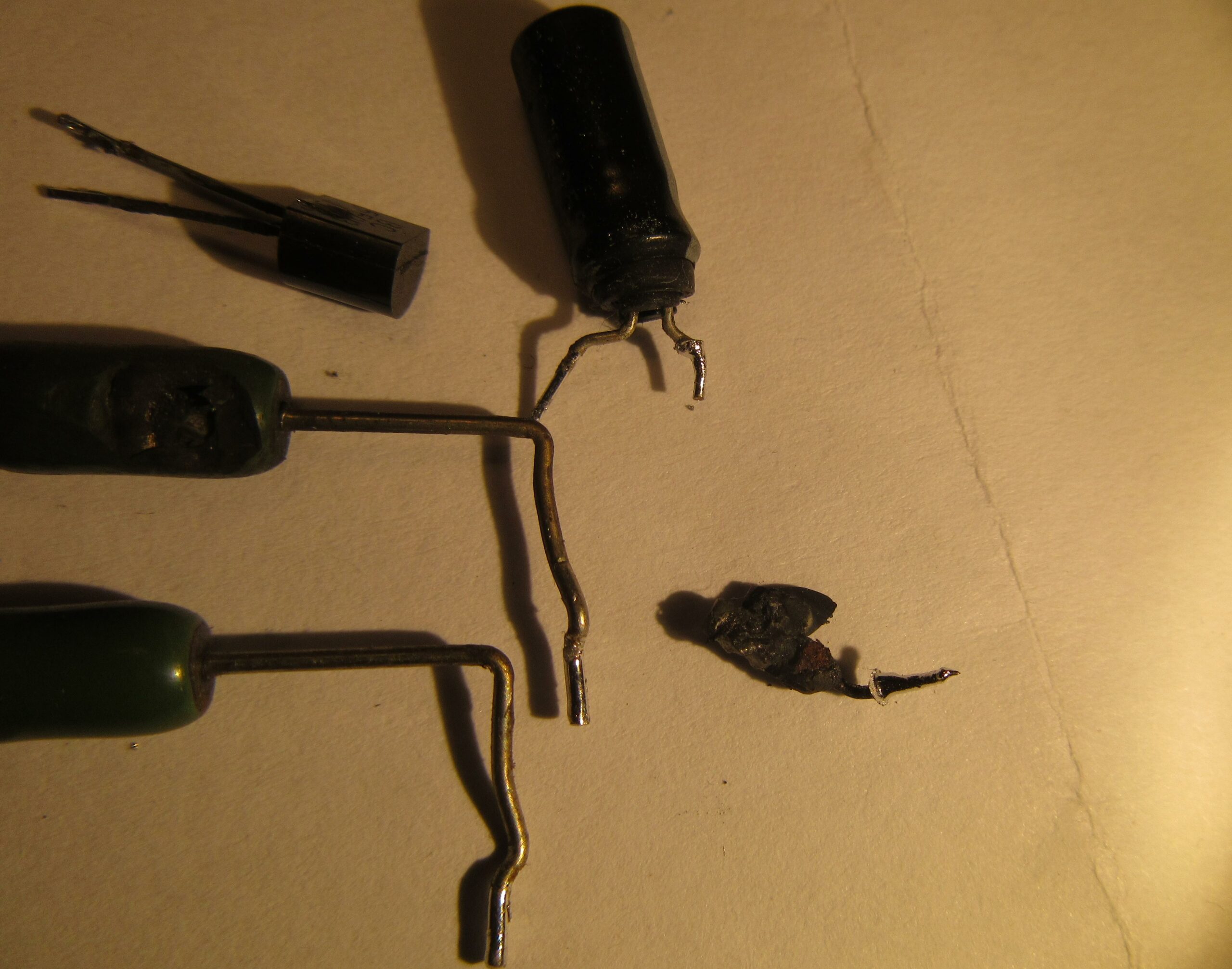
The next step was to find all defective parts and desolder them. As you can see on the photos, a lot of things came together.
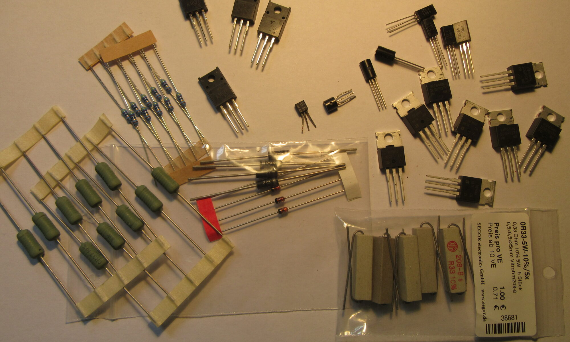
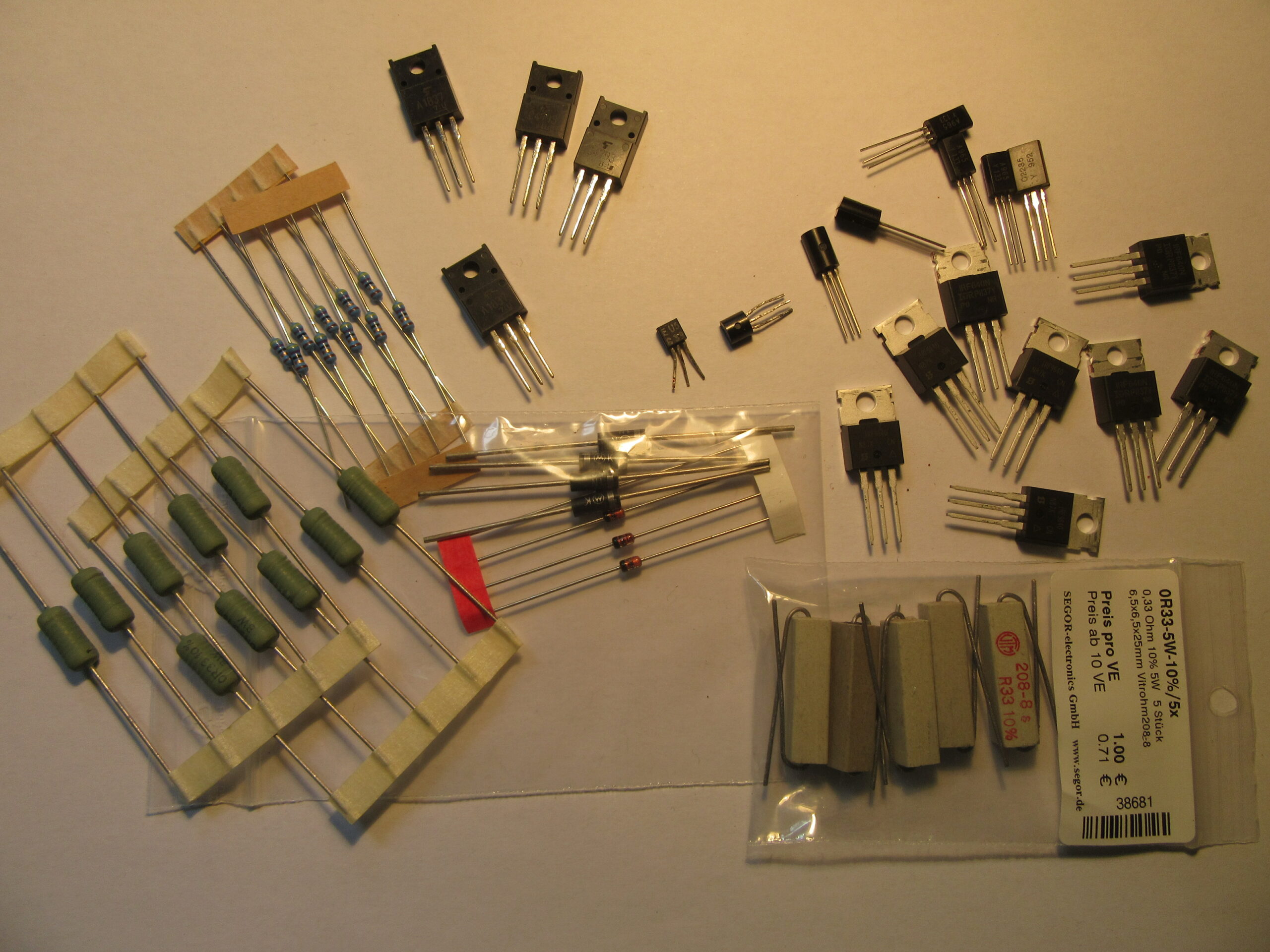
Desoldered components
Other parts

Spare parts

Getting a replacement was easy this time. My local electronics parts dealer SEGOR-electronics GmbH Berlin had everything ready, even relatively exotic Japanese transistors 2SC… were available from stock. However, I had bought the last pieces of a discontinued type.

Spares

Replacing the parts was not difficult thanks to the circuit diagram and assembly plan. After a few hours everything was done and the vaporized traces were replaced by thin PTFE-insulated wires.

Replaced tracks

Test with precautions

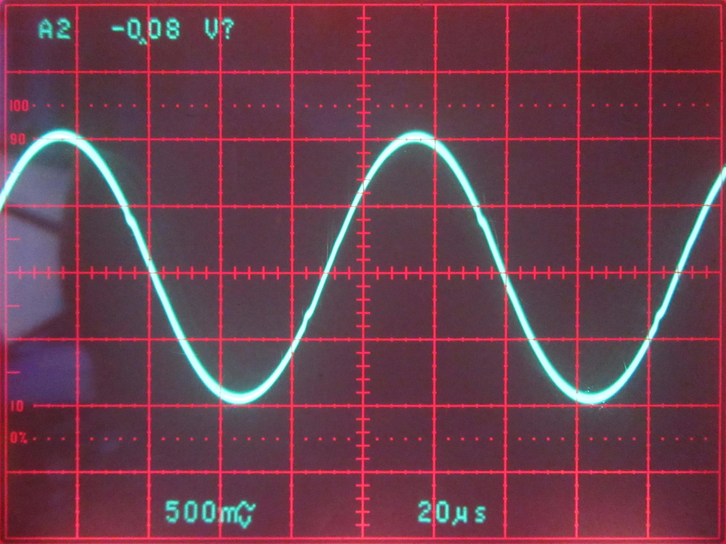
Next up was a first test. This is a delicate matter. If you’ve made a mistake or haven’t found the cause, it goes boom, little clouds rise, and you can swap various parts again. A very good insurance against a new disaster is an upstream bulb. This is looped into the power supply so that the maximum power is greatly reduced and in the event of a short circuit, for example, only the bulb lights up and nothing explodes. For a power amplifier of this size a 100W incandescent lamp is appropriate, good who still owns such a thing.

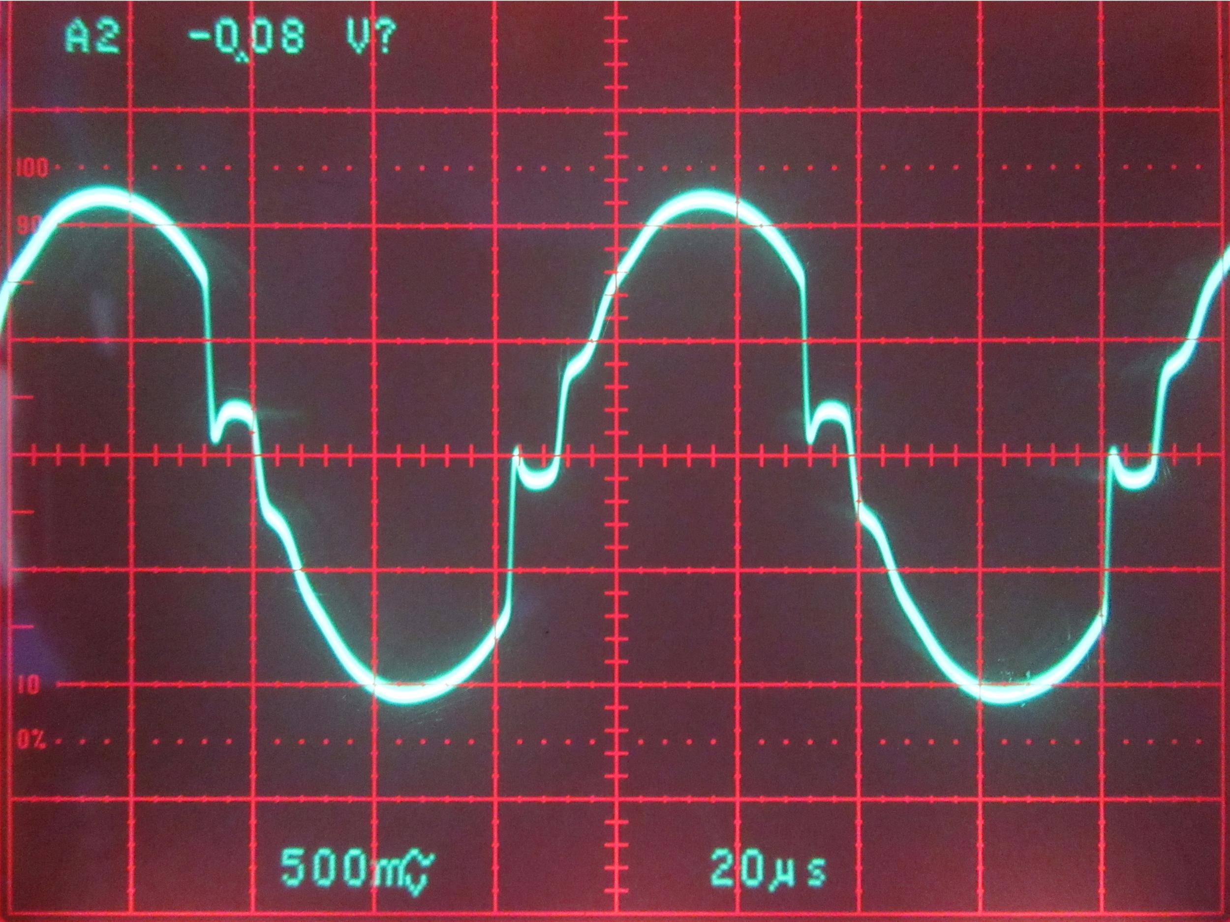
The test went well at first, the fed sinus signal could be seen at the output. However, strong distortions appeared at a slightly higher output level. The unrepaired channel still ran flawlessly.

Oszillogramm intakter Kanal
Oscillogram defective channel

Tricky troubleshooting

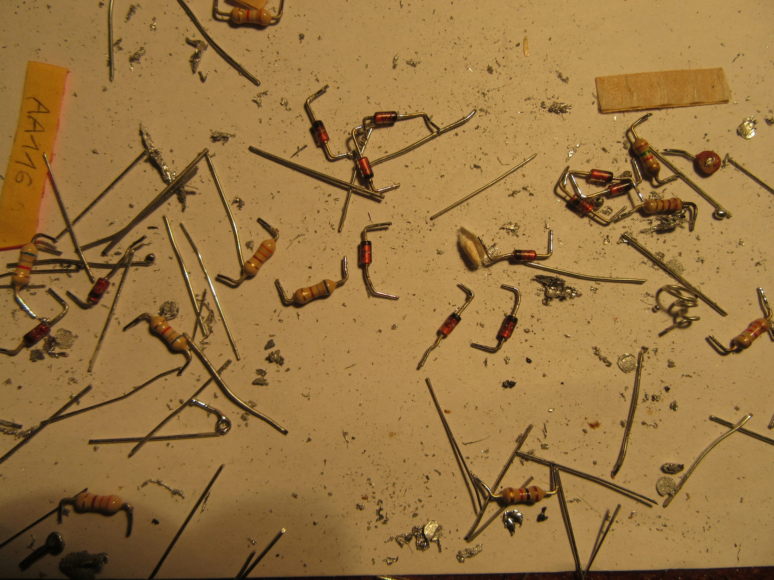
I can briefly summarize the rest of the story. During the repair of the PCB traces I had made a small mistake and connected the drivers of one half-wave with the end transistors of the other half-wave. At low volume the signal was ok, but when the end transistors take over as well, only muck comes out of the speaker. The problem haunted me for a few days. In desperation I changed almost all parts of the defective channel, without success. The unsoldered parts soon resulted in a kind of wimmelpicture.

Replaced sundries
New components soldered

After sleeping on it for a few nights, I systematically searched for the problem again. Great satisfaction when I found the tiny error and fixed it. Actually, I had done everything else right in the first attempt. That doesn’t work out very often with an extensive repair.

Adjustment

The only necessary adjustment is the quiescent current. For this I simply measured the voltage drop across the drain resistors of the intact channel and adjusted the other channel in the same way.

Error cause and update

In the test run, it turned out that the heat sinks get quite hot even without load. The built-in fans are activated at a certain temperature. The idle temperature seemed too high to me. This also matched a change or an update of the device that was in the documents K.M.E. had sent me. The update causes the fans to run permanently at low speed to prevent overheating. So now I think the cause of the defect has been found. It’s pretty sure that one of the end transistors died of heat and dragged several other components with it.

The update consisting of a 220nF capacitor and two 5.6V Z-diodes was quickly installed.

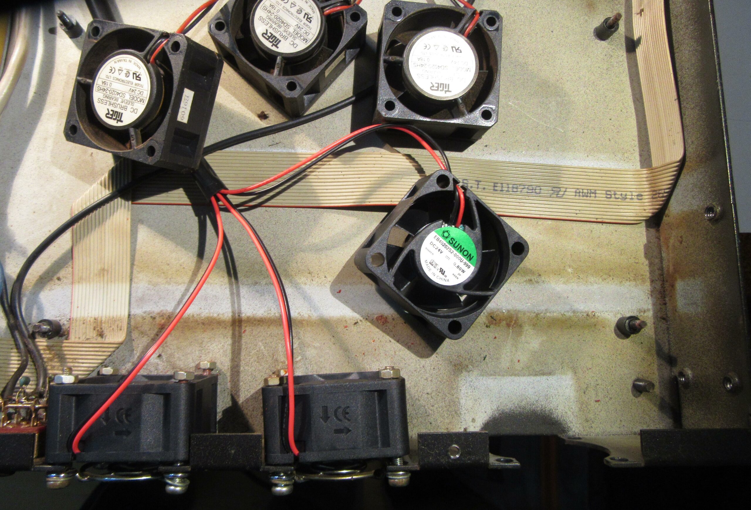
Finally, only the old, out-of-round and quite loud fans were disturbing, which are now permanently on. The quietest suitable model for replacement was quickly found and ordered.

New fan

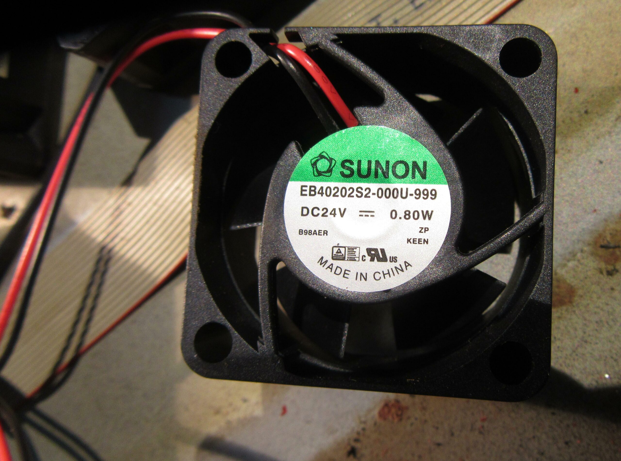
The last official act was the replacement of the three fans.

Fan replacement


Receive updates directly in your inbox

Loading

Weekend projekt: avalanche pulse generator

This project I started on a leisure weekend some time ago. The time is now to document it. Always wanted to measure the bandwidth of my two oscilloscopes, an analog and a digital one. There is help from the avalanche breakdown. During this type of breakdown, free carriers in the p-n transition region are exponential multiplied, leading to a rapid current rise. In other words, you can generate pulses with a very short rise time.

Idea

The idea I got from this article: Avalanche Pulse Generator Build Using 2N3904. The circuit is very simple but needs at least 120V to operate. Blessedly is no exotic component included like an avalanche-diode. Many standard transistors you may have in your junk box can be used for the avalanche breakdown. I found some 2N3904. Suddenly cutted a piece of breadboard, collected the remaining components and heated the soldering iron.

components and breadboard

Circuit

A old-school 555 timer IC acts as high voltage generator, a circuit I used several times before, for instance in the VU-Meter with EM84. The avalanche pulse generator itself is composed of only six components as you can see in the schematics diagram.

Schaltbild
schematics

Construction

Initially I tried with the 2N3904. My transistor batch purchased from SEGOR-electronics GmbH Berlin had an avalanche breakdown at 130V. At this shop I purchased some 2N2369A too which had the breakdown at about 90V. For this project the 2N2369A is a better choice and I like the vintage TO18 metal case. Depending on manufacturer and production date I suspect a large variance in the avalanche breakdown voltage of different transistor lots. So you have to experiment a bit to find a good matching part.

put together

Shortly the small circuit was assembled and operated at the first go. Excitedly I awaited now the bandwidth check of the oscilloscopes. There is no formula definition to calculate bandwith from rise time. Usually the bandwidth is calculated with 0,35 divided by rise time. The rise time is the time meanwhile the signal grows from 10% to 90% of the maximum.

Oscilloscope tests

First in turn was the good old analog Tektronix 2465B. (1991 model)

bandwidth test TDS2465B

The screen has markers at 10% and 90% and a cursor for Δt which makes it easy to adjust the trace and read out the rise time. The determined 0.78ns rise time is equal to a bandwidth of about 450MHz. This is distinctly more than Tektronix guarantees, I’m satisfied.

Next in turn was the digital TDS784C. (1996 model)

TDS784C rise time

The device can measure the rise time automatically. The result is fairly exact 1GHz bandwidth, as the manufacturer says. Interesting for me was the fact that the signal rise stopped at about 10% for some time and grows very fast later as you can see better with a zoomed x-axis.

rise time detail

Case

Summa summarum all went as expected and I learned some things. In the end the circuit got a cute case at this time labelled indeed.

Receive updates directly in your inbox

Loading

dsPIC33 Experiments


Anyone who has read my article “Weekend project: bat detector” will have heard, that I was not fully satisfied with the result. The device is working but it’s too insensitive. This induced me to start from scratch and build it again. This time with digital technology which is better prepared for the task. The electronic key component is a dsPIC33E, a microcontroller with DSP functions from Microchip.

The Goal

The idea is to record the ultrasonic signal with microphones which are sensitive in the needed frequency range. Subsequent the amplified signal will be AD-converted with a sampling rate of 300kHz at least. After a spectral analysis with FFT the spectrum is indicated at a display. If possible the signal will be rendered audible by an inverse FFT after changing the sampling rate. This procedure should transform the gamut of the signal to lower frequencies, hearable for humans. As far as this coarse ideas become real and the project grows with all hardware, software and mathematics, I will certainly write something about it in this blog.

The Experiment

Initially I need a small system for digital signal processing. A preamp and signal conditioner at the input, AD-converter, a DSP or a fast microcontroller and at the end of the chain a DA-converter. The system shouldn’t lack a small display too. Nice to have would be a battery power supply and additional supply by USB.

block diagram with front end, AD-converter, DSP, DA-converter and power supply

Component Inquiries

Every time a project like this one starts with investigations on the components to use. Which microcontroller will be chosen, what kind of converters to use, how to build the power supply et cetera. These considerations leads to a pretty detailed block diagram as shown above.

Unfortunately some special components are not sold in small quantities and often only an B2B (business to business) selling platforms or with very high shipping costs. The DSP for instance I had to order as a sample directly at the manufacturer. At all I needed to place 3-4 orders. Because of SMD cases of some chips I had to solder these on small adapter boards to use the chips in my hand soldered prototype design on a stripboard.

adapter boards for several TSSOP and SSOP cases

Prototype

The orders arrived and some tinker evenings later the prototype was ready for some tests. I always do this step by step for each component.

prototype built on stripboard

Starting point was the oscillator, followed by the I2C bus, the OLED display and the AD/DA-converters. At this step I faltered. Every time it is fiddly to bring an SPI (synchronous serial interface) to work, especially at high data rates and if the default configuration of both sides does not match. To solve the problem I had to buy a new logic analyzer with 100MHz resolution. Root cause was the need of a signal /CONVST (conversion start) to trigger a conversion at the AD-converter. The CPU wasn’t able to generate this signal fast enough and especially not synchronous. As a way out I used the inverted signal /SS (slave sync) of the SPI as /CONVST. Conversions should anyway run synchronous to the SPI transfers which implies one transfer (/SS) follows one conversion (/CONVST).

To analyze the electrical signals during data transfers I use PulseView, an awesome open source software for logic analyzers including some amazingly cheap devices like Cypress EZ-USB FX2 based ones.

logic analyzer readout for SPI-interface of the MAX8328 AD-converter

After sailing around some difficulties with hard- and software it was a terrific moment to hear the first synthesized distortion free sinus tone.

Software

The software is mainly written in C. An integrated development environment, “MPLAB® X“, is provided by the CPU manufacturer which is freely available but has some limitations. More than an “-o1” is not allowed and leads to comparatively slow code. This is no problem at all here, time-sensitive parts are simply implemented in assembler.
By the way a tip for all users of GCC, AVR-GCC etc: It’s quite easy to integrate assembler code in C. Just add a file with “.s” or “.S” extension to the project and add your assembler code there. The file with the capital s extension will additionally handled by the preprocessor.

The latest version of the software is published on my Github-Account.

Hardware

The hardware is not yet perfect but good suited for further experiments. After all the system is able to process the input with 16bit at 384kHz mono or 192kHz stereo sample rate and output simultaneously 24bit at 192kHz stereo sample rate. At the same time the CPU is busy by a few percent only due to DMA transfers.

schematics, still without front end for microphones and line-in

Anyway for the next prototype some things I will improve, primarily to simplify the SPI programming.

  • dsPIC with I2S interface
  • dsPIC with at least 3 SPI interfaces and more IO ports
  • bigger and colored display
  • additional RAM, may connected to SPI port

More RAM would be great. The maximum on chip memory for dsPIC33 CPUs is about 50kBytes. A dsPIC33EP512GP806 in a TQFP64 case could be a good fit, a 32bit controller like the PIC32MZ1024EFH100 might be an excellent choice too.

preliminary finished evaluation board with programming adapter and logic analyzer in operation

Receive updates directly in your inbox

Loading

Weekend project: bat detector

Since ages I observe lots of bats in the evening and I’m interested in there specific style of orientation and communication. Two weeks ago I had some leisure time to build my own bat detector.

I wanted to build a prototype on a stripboard only and investigated to find a premade circuit. A short internet enquiry showed up a bunch of instructions. After some reading and checking my stock of components I decided to go for a simple analog circuit built around one 4xOPV LM324N.

block diagram

The principle is similar to a superheterodyne receiver. The high frequency input is amplified by about 140.000x and mixed with an oscillator signal to an audible frequency range. The concept of a frequency mixer is comprehensive described at Wikipedia. I implemented only a few modifications in the circuit. So I replaced the 62kΩ resistor in amplifier stage two with an 68kΩ type which increased amplification marginally. Additionally I used a 100kΩ potentiometer because I hadn’t a 50kΩ pot available. The entire circuit without the modifications is available here:


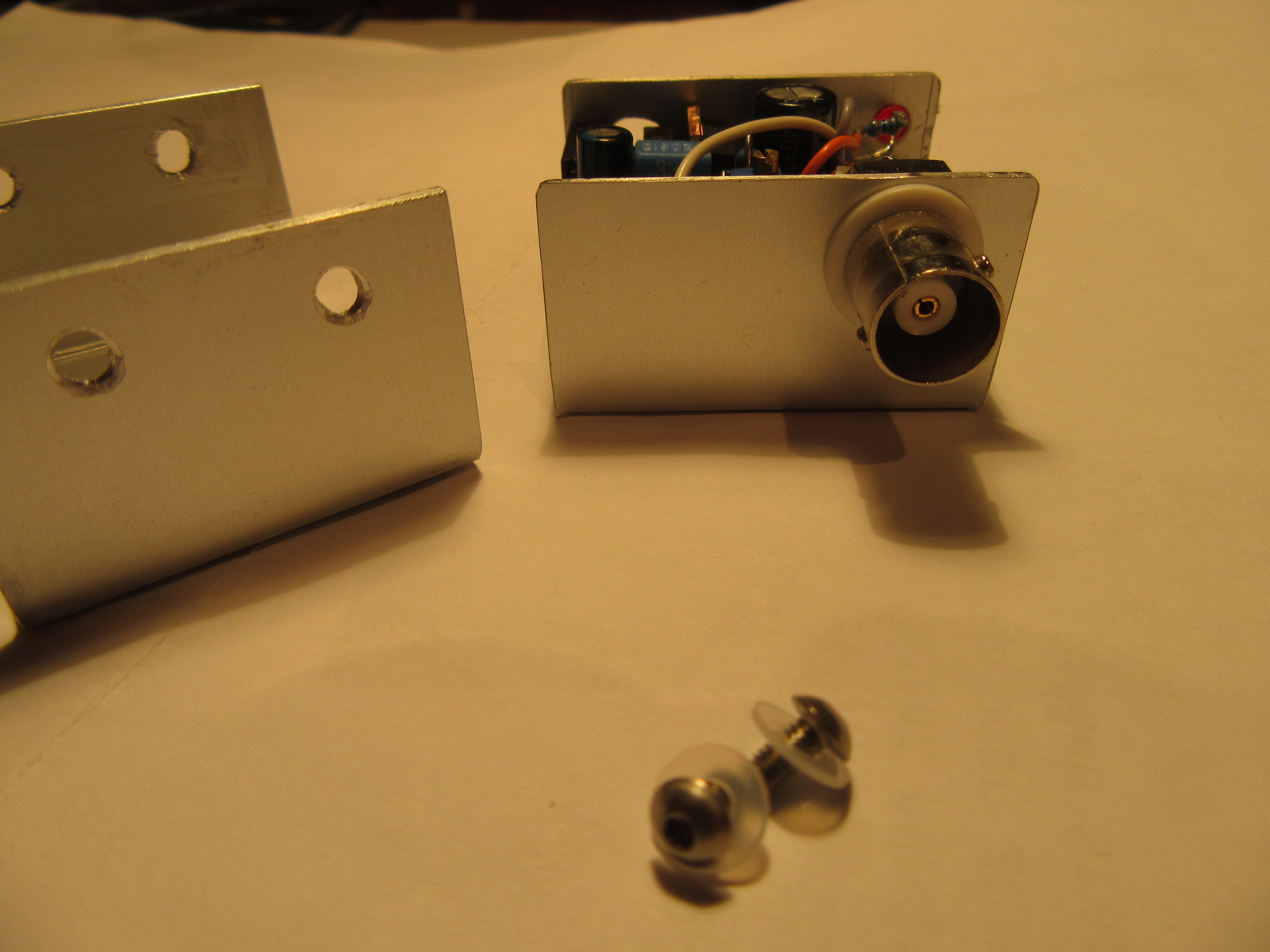
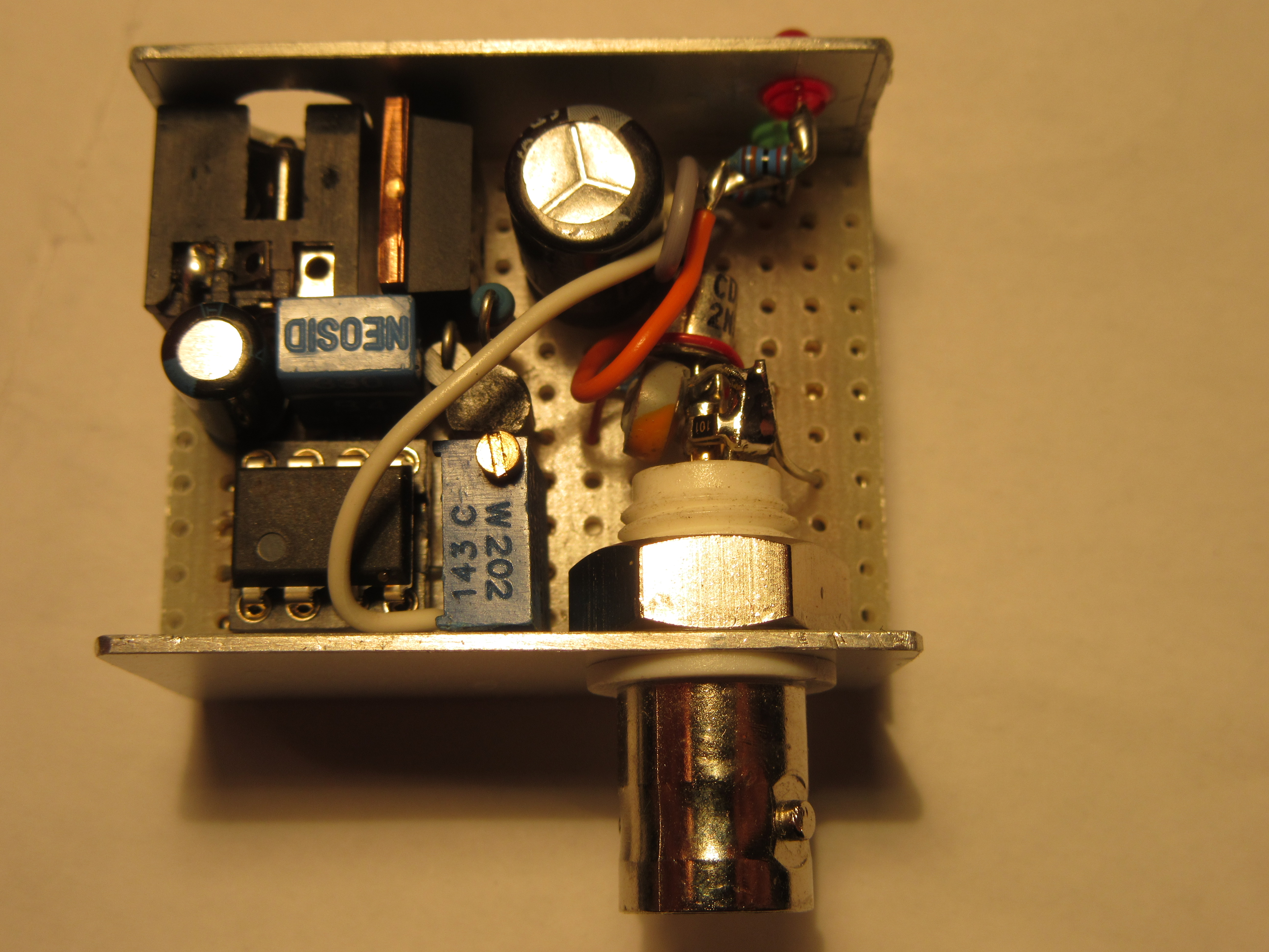
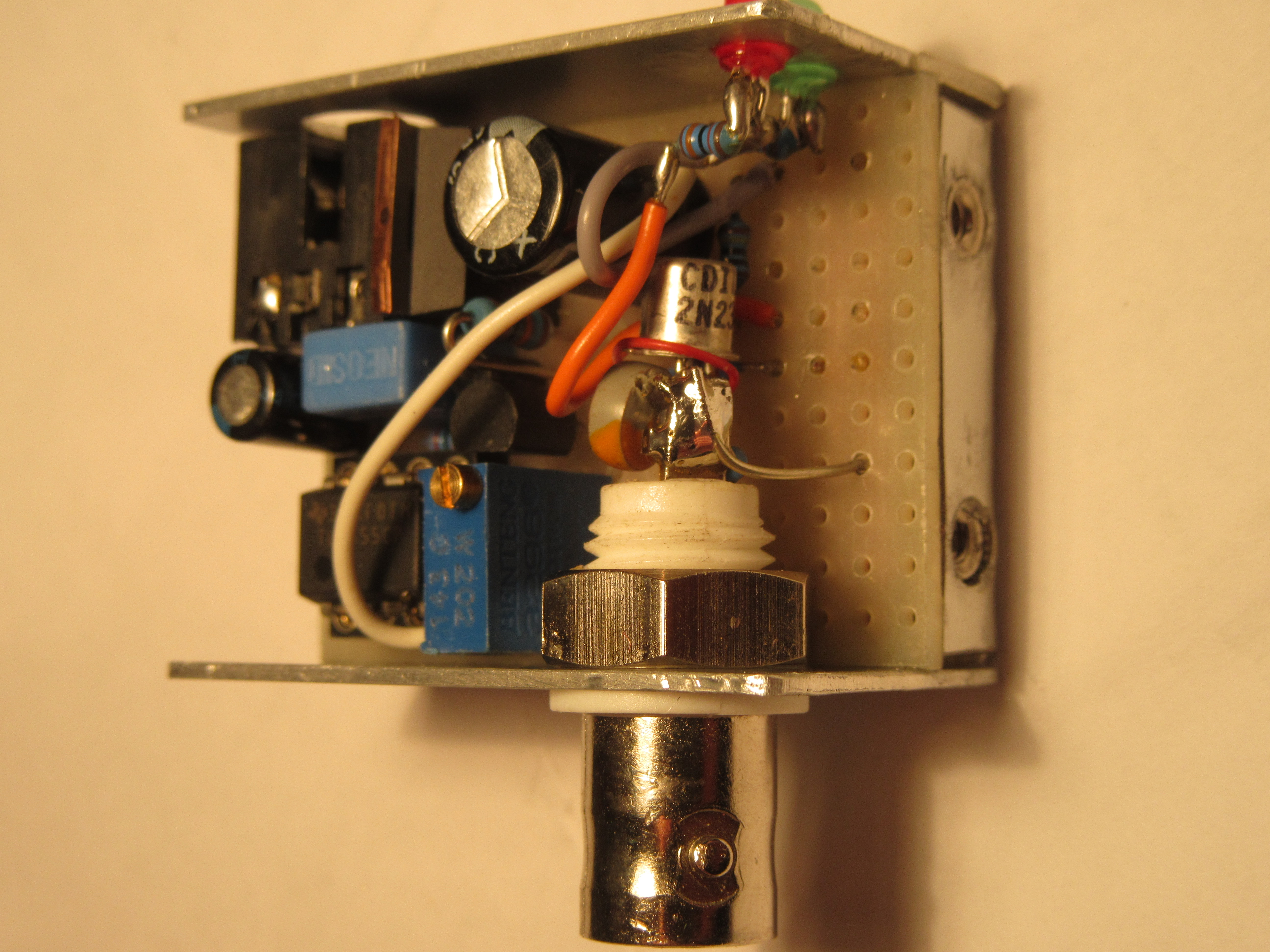
Bat Detector, Source: https://www.nutsvolts.com/

The abovementioned page marvellous describes some background information about bats and the detector which are essential. To use the detector right it’s needful to read the article.

Hereafter is a small picture story that shows the construction. Because I liked the project I designed an adequate chic case from plywood. The microphone is pluggable to allow experiments with different devices.

case parts, gummed up and oil treated

assembly done

stripboard top view

stripboard bottom view

battery compartment

ready for service

microphone (piezo buzzer)

The first trials indicated that patience is needed to hear a bat. The noise is soft and it can can only picked up if the mammals heading is towards your position. In a patio in Berlin where five to ten bats circling during dusk you luckily hear every quarter hour a kind of rhythmic giggle.


Receive updates directly in your inbox

Loading

USB load cell interface with AD7797

This project I developed and published first in 2011, years ahead many other similar proposals. It is a well-structured approach with good working and free available software to connect a load cell with USB. I used a cheap kitchen scale for 10 Euros to create an USB scale with a resolution of less than 1g.

foto of the prototype, a load cell from a 5kg kitchen scale on the left

Part 1: USB load cell interface controller

Heart of the hardware part is an Atmel ATMEGA644 microcontroller. The controller manages the A/D conversion and reads the results from the AD7797. On the other side the Atmel acts as a low speed USB 1.1 HID device with the advantage that no extra USB driver is needed in the operating system where this circuit is connected to.

Additional functions are provided by the microcontroller like automatic conversion, offset calibration and some statistic calculations. These calculations include mean, median, variance and standard deviation. The statistical base is user defined from 2 to 256 values. Useful debug output is also available at the RS232 interface connected to the ATMEGA644 UART. You have to set the “DEBUG” flag in the firmware source code and recompile to make use of this feature.

The USB part of the firmware uses V-USB, a firmware-only USB driver from Objective Development Software GmbH.

The software for the integrated microcontroller ATMEGA644 is available for avr-gcc. It is written in C and developed with “AVR Studio 4.18”, SP3, an IDE for 8-bit AVR-controller by Atmel. The latest source code is provided under the GNU General Public License (GPL) and can be downloaded here.

Part 2: front end

The front end for the load cells measurement bridge consists of the 24 bits A/D-converter AD7797 from Analog Devices with an integrated amplifier with a gain of 128. So the A/D-converter can be directly interfaced to the load cell without additional amplifier. The reference voltage is generated by an ADR441 ultra low noise voltage reference, also from Analog Devices.

The front end can be offset and gain calibrated. These parameters are stored in the controllers EEPROM and loaded at power up.

close up of the circuit, RS232 debug interface left top, the A/D-converter bottom right

Part 3: USB Host Software with GUI

I wrote a software example for Linux and Windows and possibly for MacOS which demonstrates USB HID programming and all of the circuit functions. It is written in C++ and developed with “Qt Creator”, a Cross-Platform Qt IDE by Qt Software and Nokia Corporation. The source code is provided under the GNU General Public License (GPL) and can be downloaded here.

Precompiled program binaries can be downloaded here for linux/x86_64 and win32.

screenshot measure

calibrate functions

statistics

project goals

  • 24 bits A/D-converter, 21 bits effective resolution
  • integrated statistics functions
  • EEPROM stored calibration and startup parameters
  • USB HID device – no extra device driver needed
  • optional debug output
  • multi platform graphical user interface
  • unique USB id: vendor: 0x16c0, product: 0x05df, Manufacturer: “runlevel3.de”, Product: “USB-A/D-Interface”

The schematics is available for download here.

USB-AD-Converter_schematics.pdf


Receive updates directly in your inbox

Loading