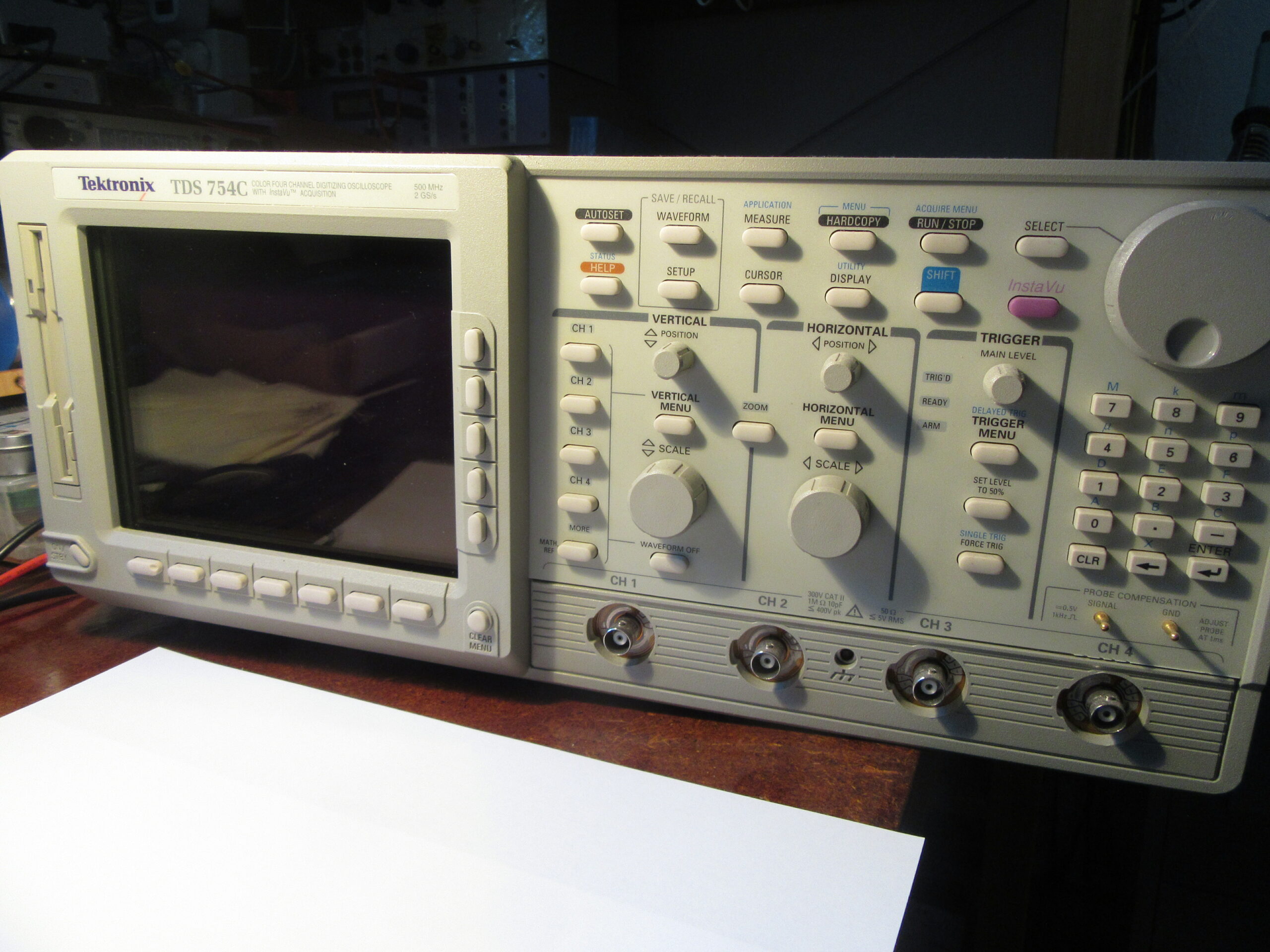
Finally there was a day off at the weekend. This time I wanted to use it to perform a maintenance on my Tektronix TDS754C digital oscilloscope that had been pending for years. The plan was to replace the two ICs from “Dallas Semiconductor” with integrated lithium battery. And that before they fail and lose all data. After 24 years. There is no more time to waste.
Preparation
The preparation for this maintenance started years ago and took a long time, as it is with hobbies. Two things I had to do in advance:
- Upgrade my homebrew programmer to 4MBit and make it able to read and write FRAM and NVRAM chip types.
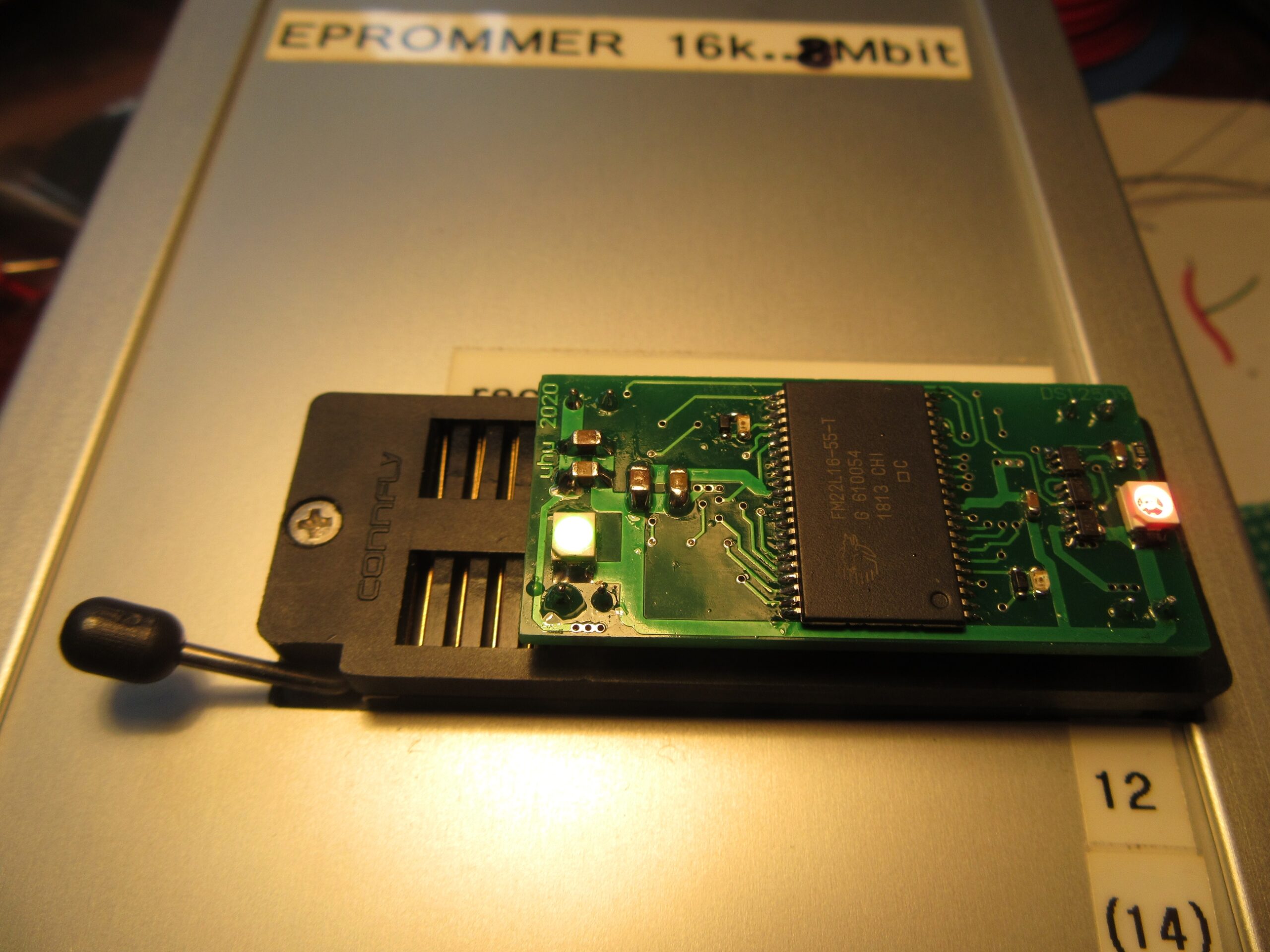
- Building a replacement for DS1250Y or DS1650Y chips.
I had already finished the extension of my programmer in 2018. I was able to check off the second item this spring and have described it in detail here.
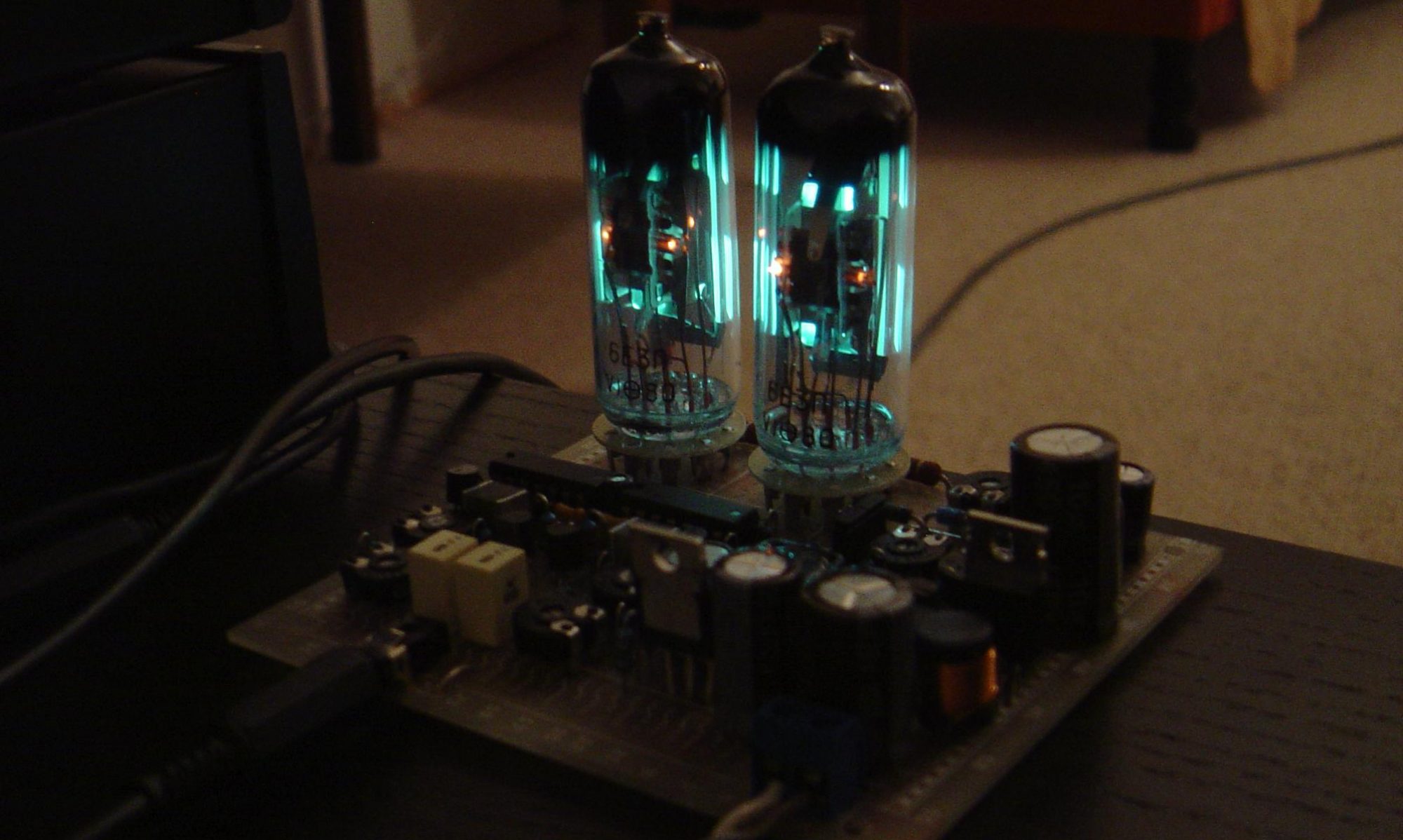
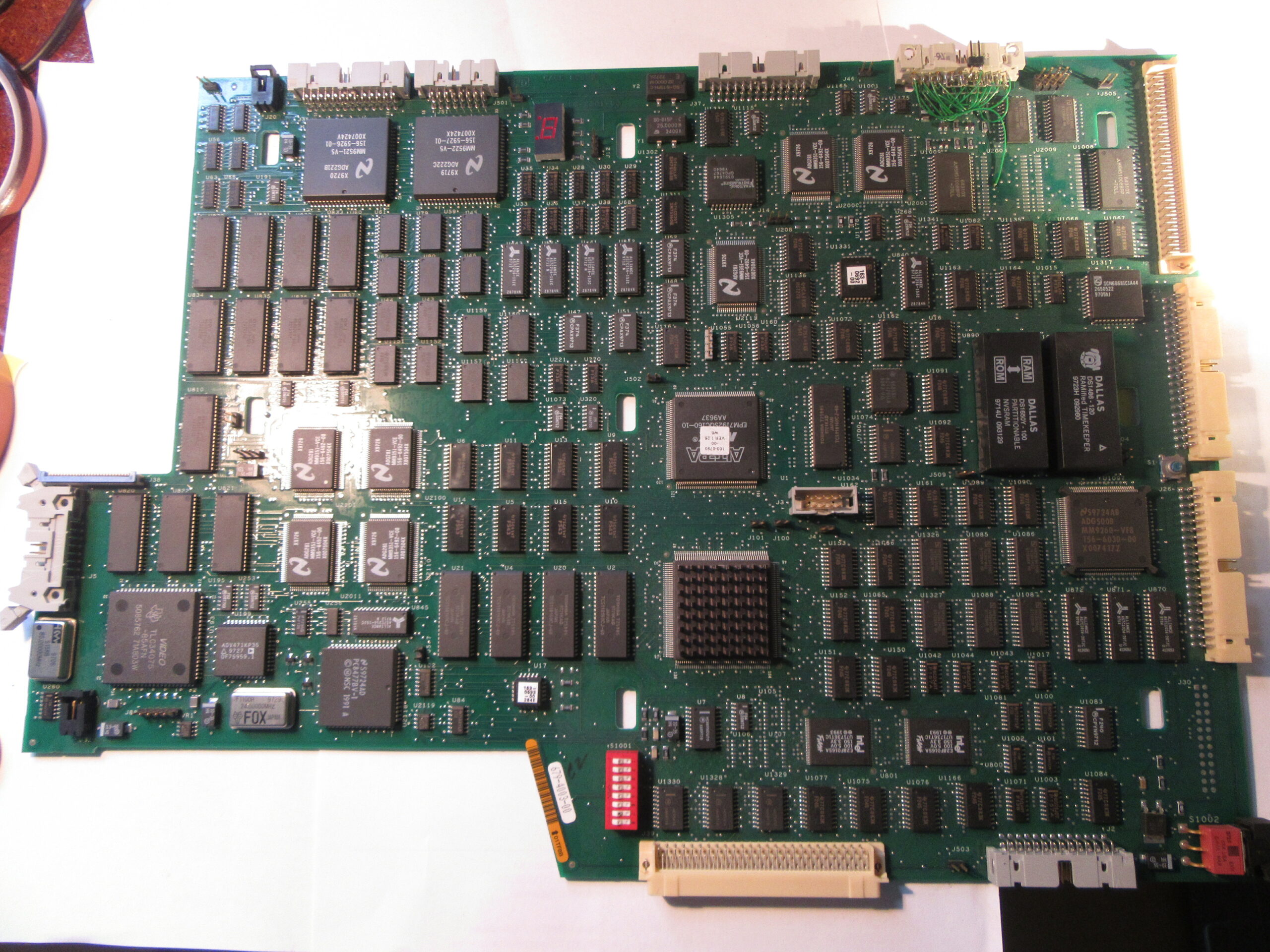
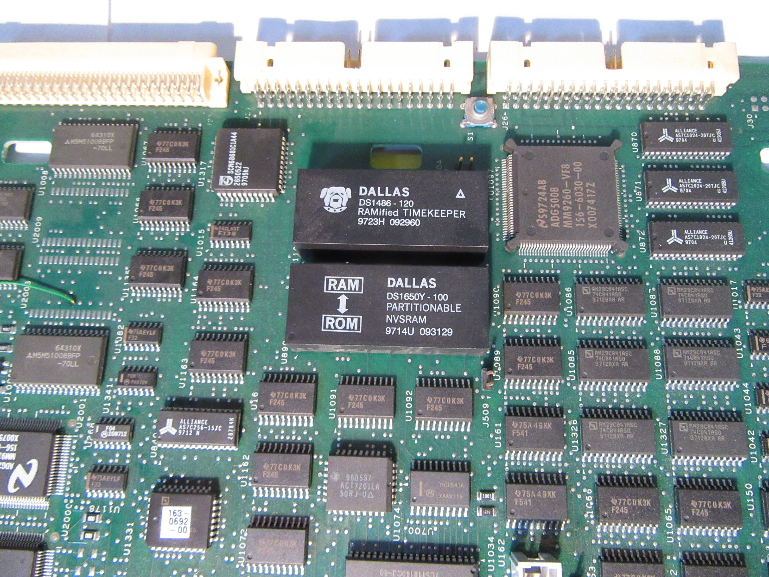
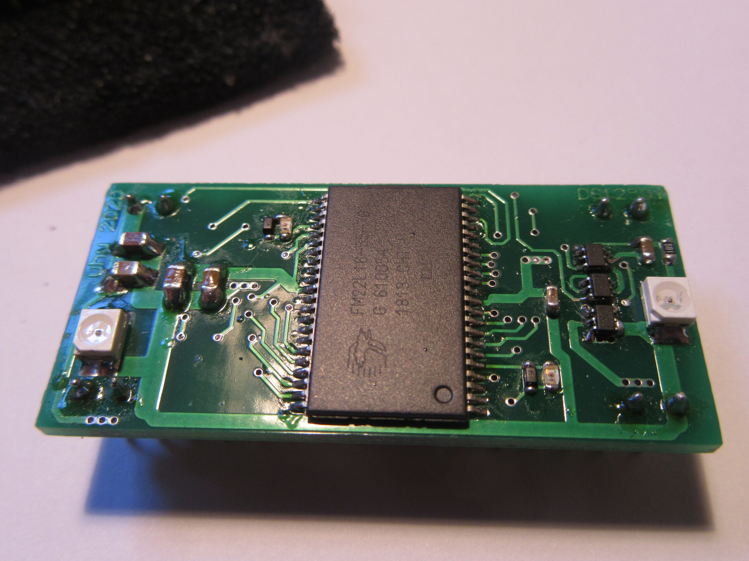
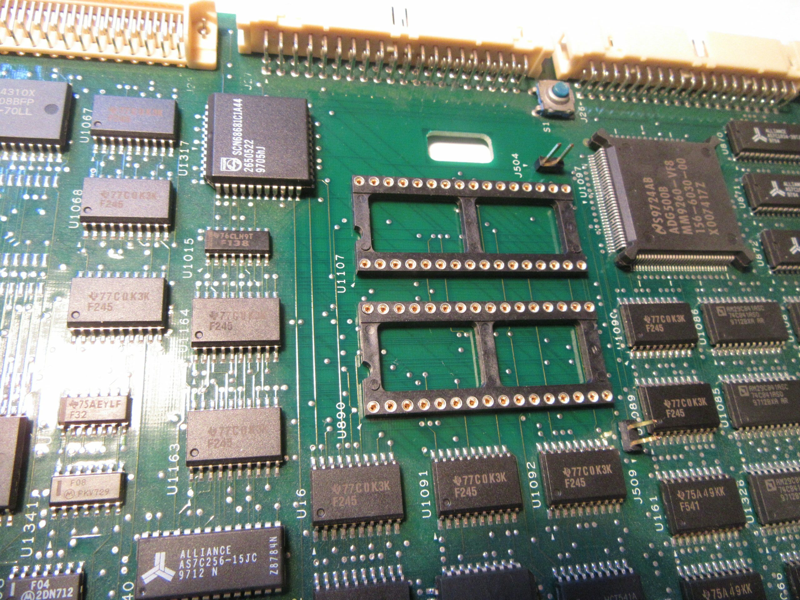
There are two of these ticking time bombs installed in the device, Dallas chips with integrated Lithium battery. I also described the problem with these components in more detail in this article. Specifically, it is a DS1486 RTC+1MBit NVRAM and a DS1650Y 4MBit NVRAM, both of which are soldered onto the CPU board.
In the case of the oscilloscope here, a failure of the two ICs would mean that calibration data and information about enabled additional functions would be lost. After all, the built-in batteries lasted from 1997 to 2021. With ten years of guaranteed life, that’s almost two and a half times the time.
Data backup
First, it’s a good idea to make a backup of the NVRAM contents. The device has a built-in 1.44MB HD floppy drive. Fortunately, someone wrote some scripts and posted them here that allow you to back up the NVRAM to a floppy.
For me the whole thing worked flawlessly on the first try. I used the tool “tdsNvramFloppyDumper”. Later I used the programmer to write the data to the replacement chips.
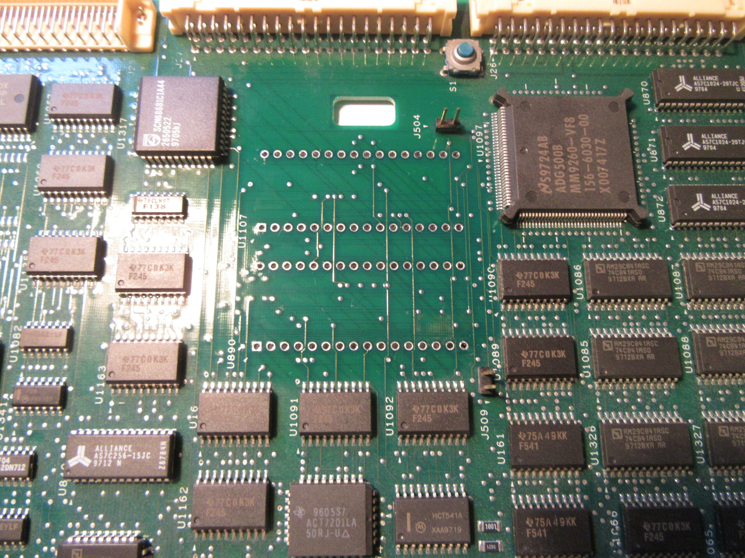
Desoldering
Now it was time to desolder the old parts. The oscilloscope is built very service friendly. To remove the CPU board, no instructions are necessary in my opinion. The desoldering itself I always do with this somewhat larger manual desoldering pump and a normal electronic soldering iron.
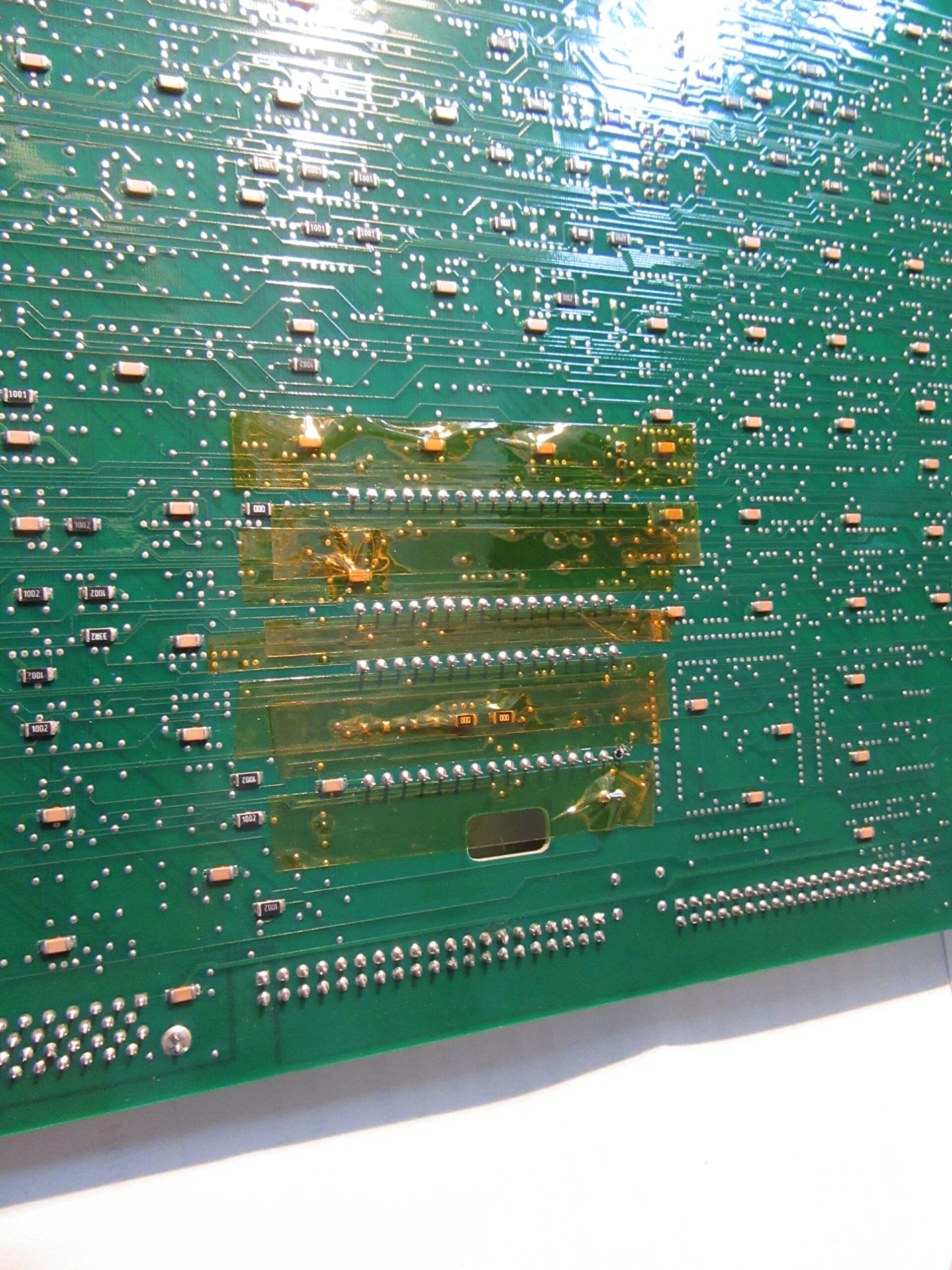
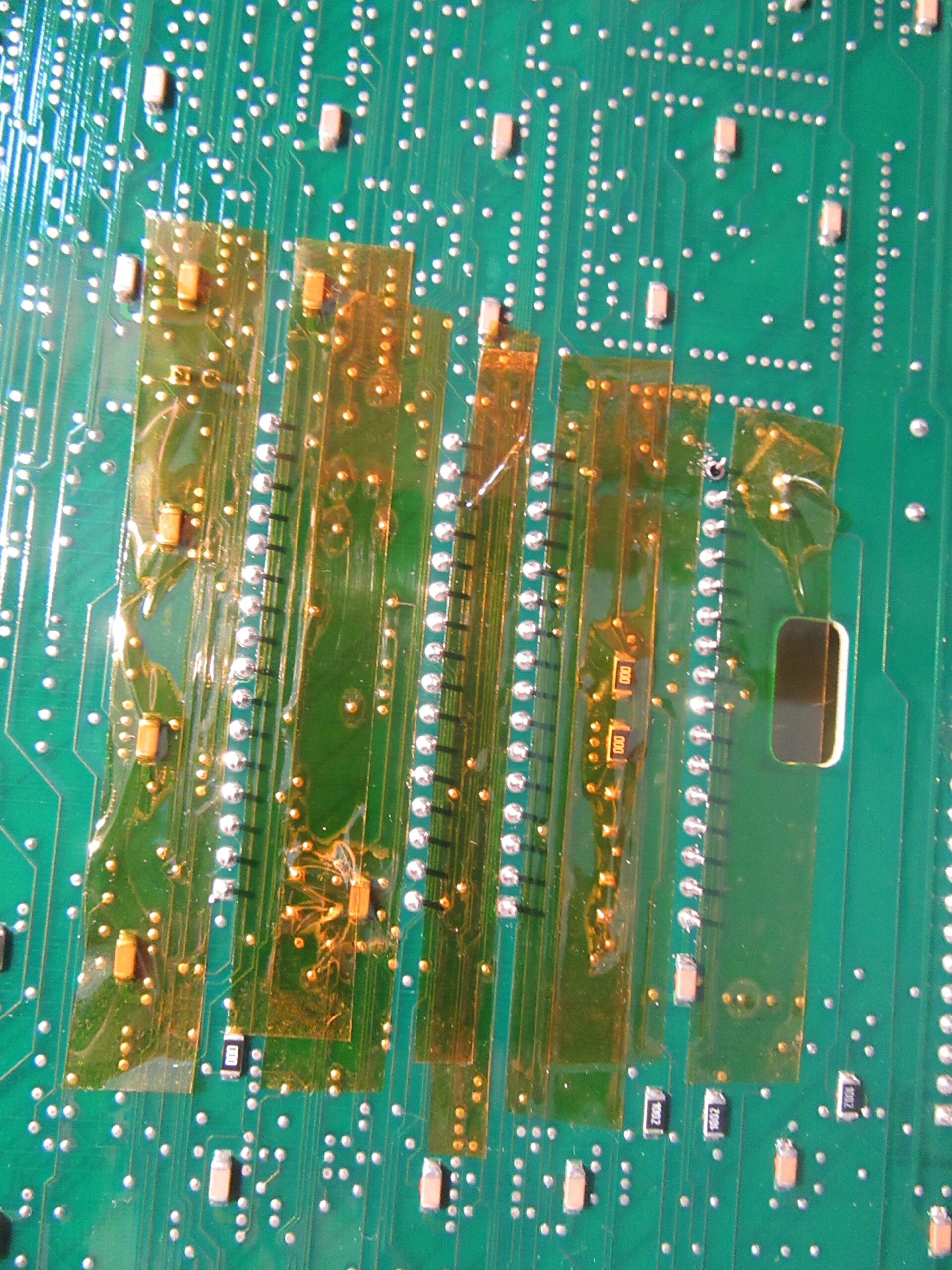
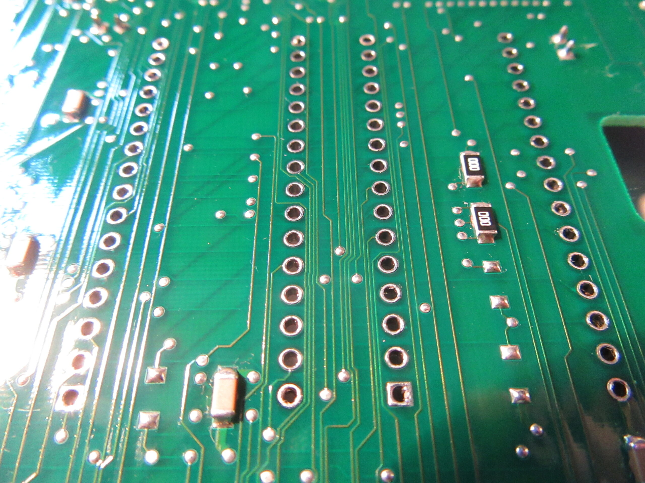
It is important to protect adjacent thin conductors with Kapton tape. The recoil of the pump throws the soldering tip a little bit away when triggering. This occasionally destroys thin conductors next to the solder pads. The tape reliably prevents this in my experience. The desoldering worked fine, I also had only one attempt.
Exchange parts
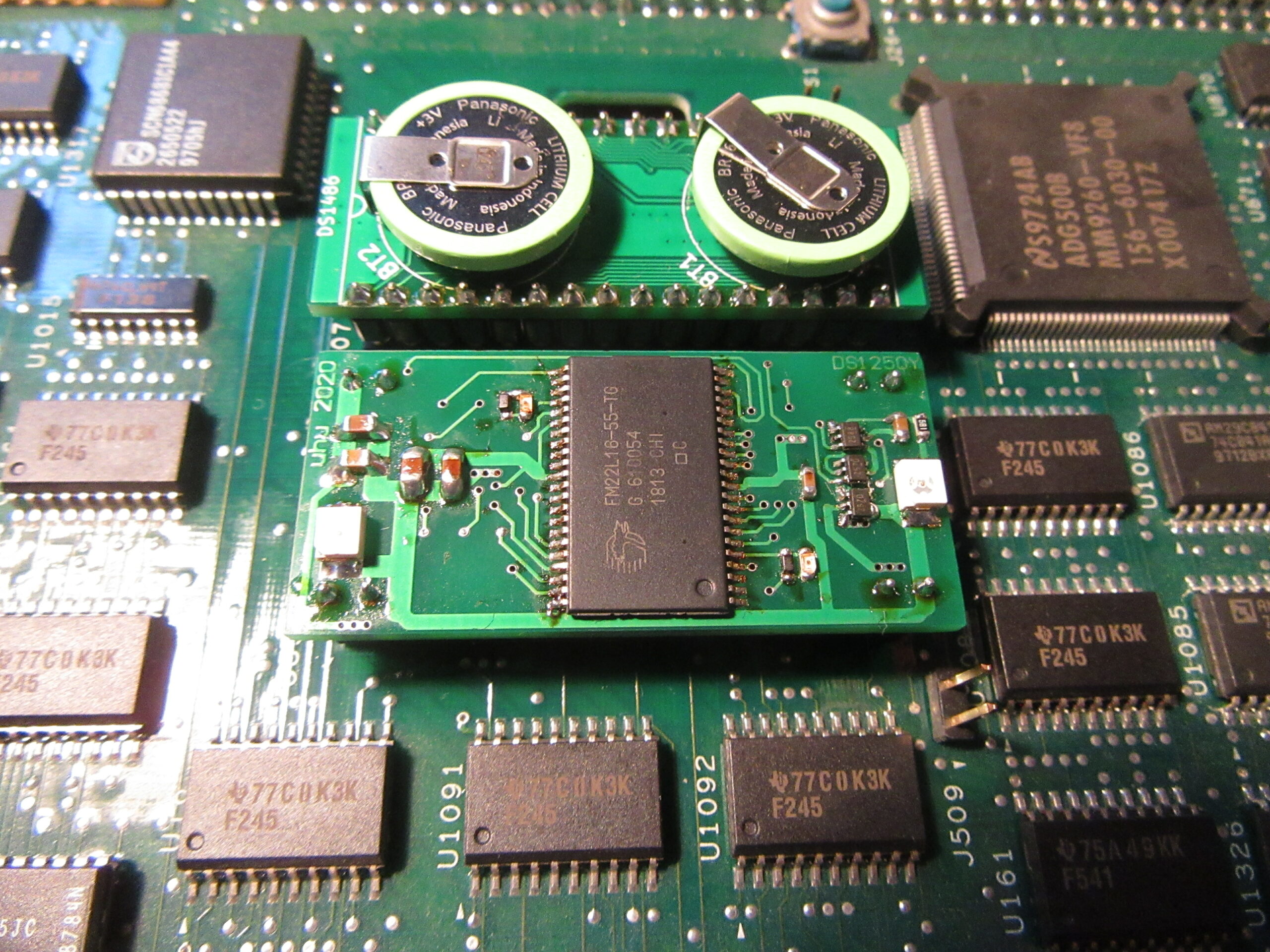
DS1486
The RTC is the more difficult part. I was lucky and found a ready-to-use rebuild instructions on the net as well as a remaining stock seller from China, who sells the obsolete DS1384G, which is necessary for the replacement. Nevertheless, be careful with the purchase, also from this IC all kinds of fakes are traded.
Rebuilding the small module was easy. During testing I learned that both batteries must be connected for the RTC to work. At first I had tested this only with the primary battery.
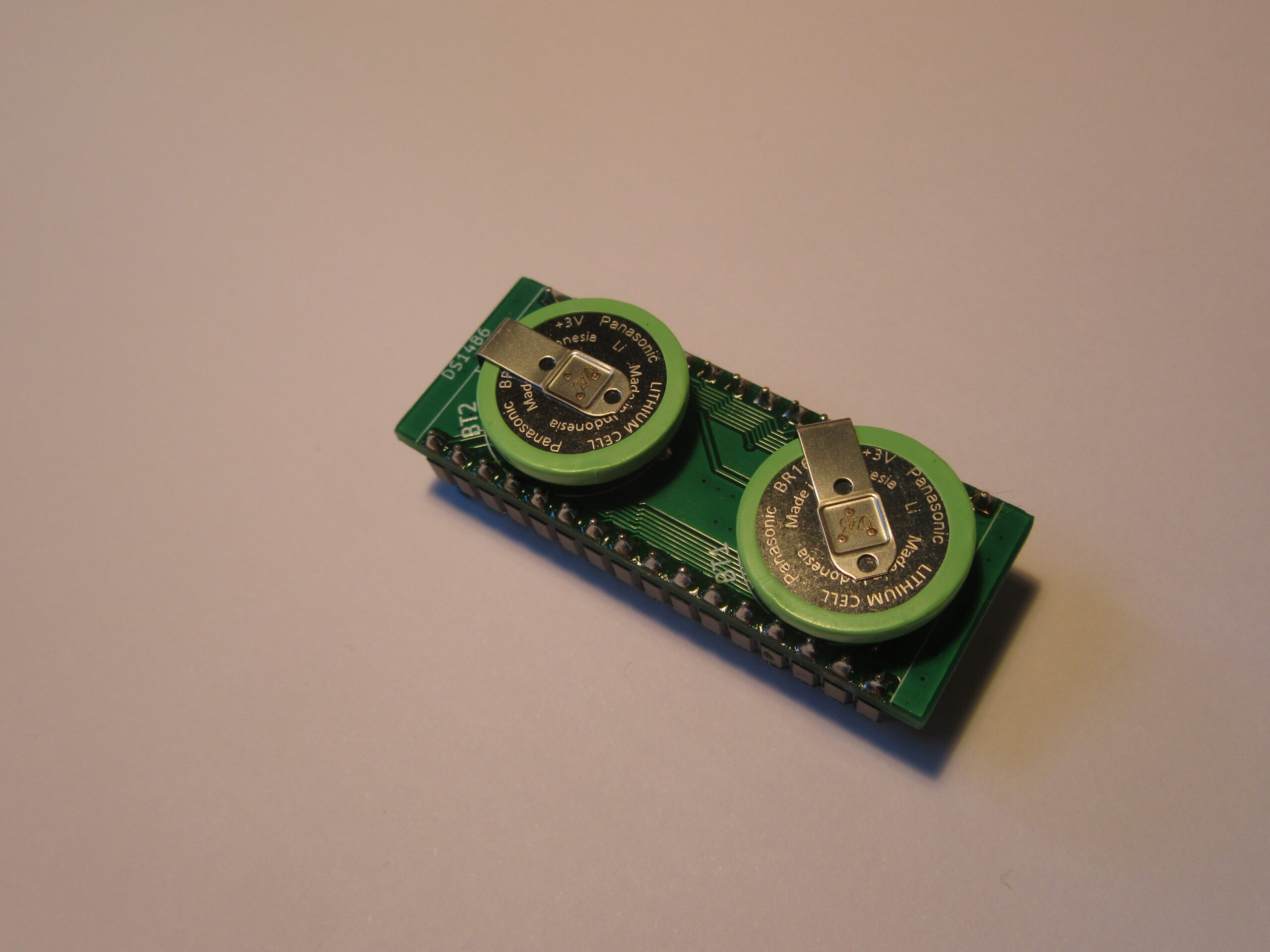
Another thing worth mentioning is the choice of batteries. There are six different common lithium battery technologies and some exotic. All have different voltages, advantages and disadvantages. In this case here it is important that the self-discharge is low and the capacity is high. This guarantees a long service life. The type “BR1632A/HAN” from Panasonic used here is a lithium carbon monofluoride battery, which meets these requirements.
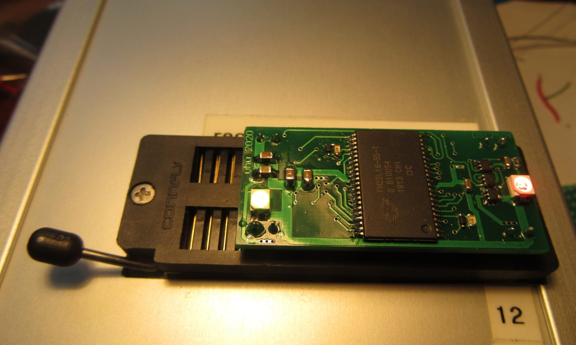
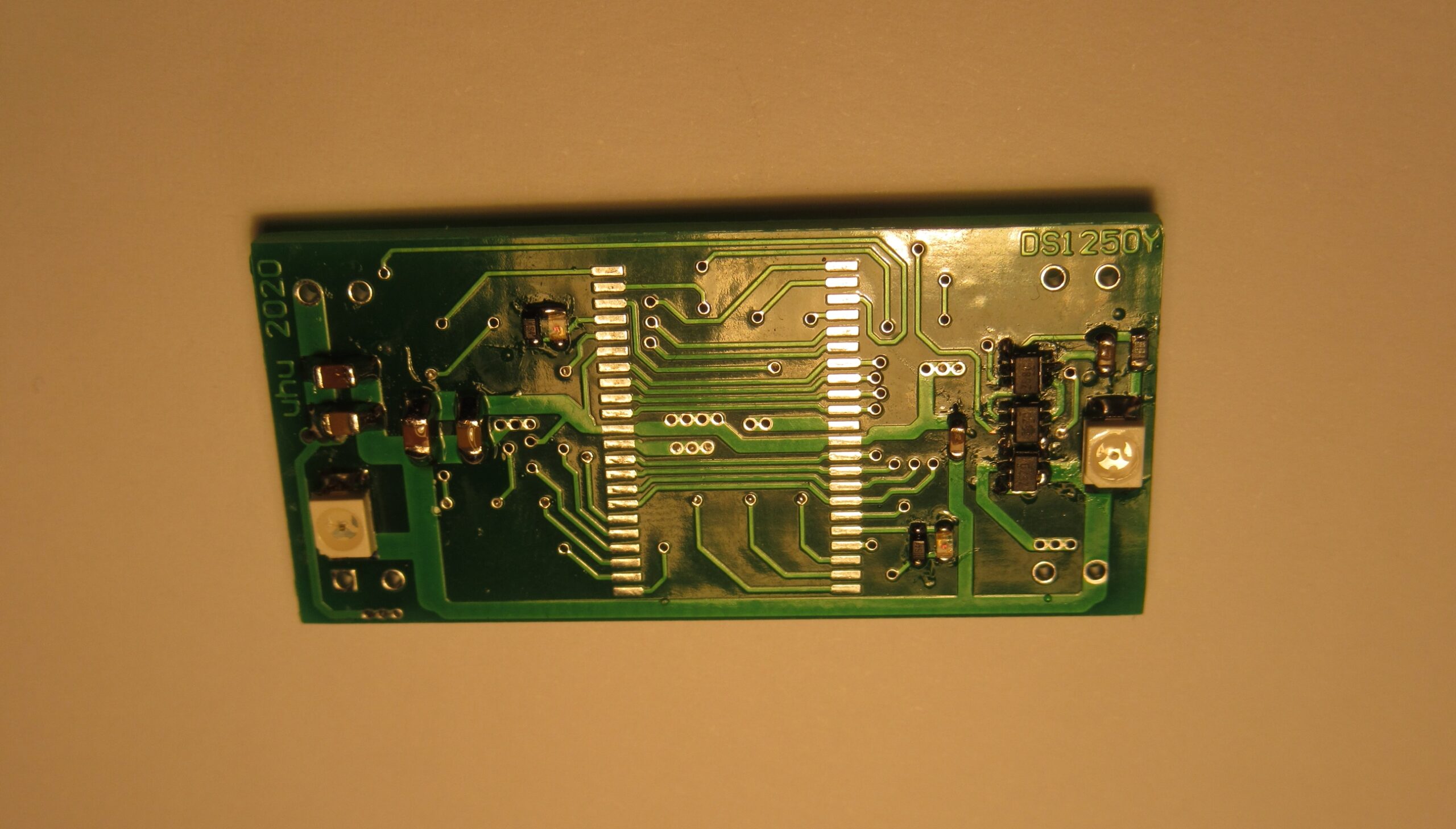
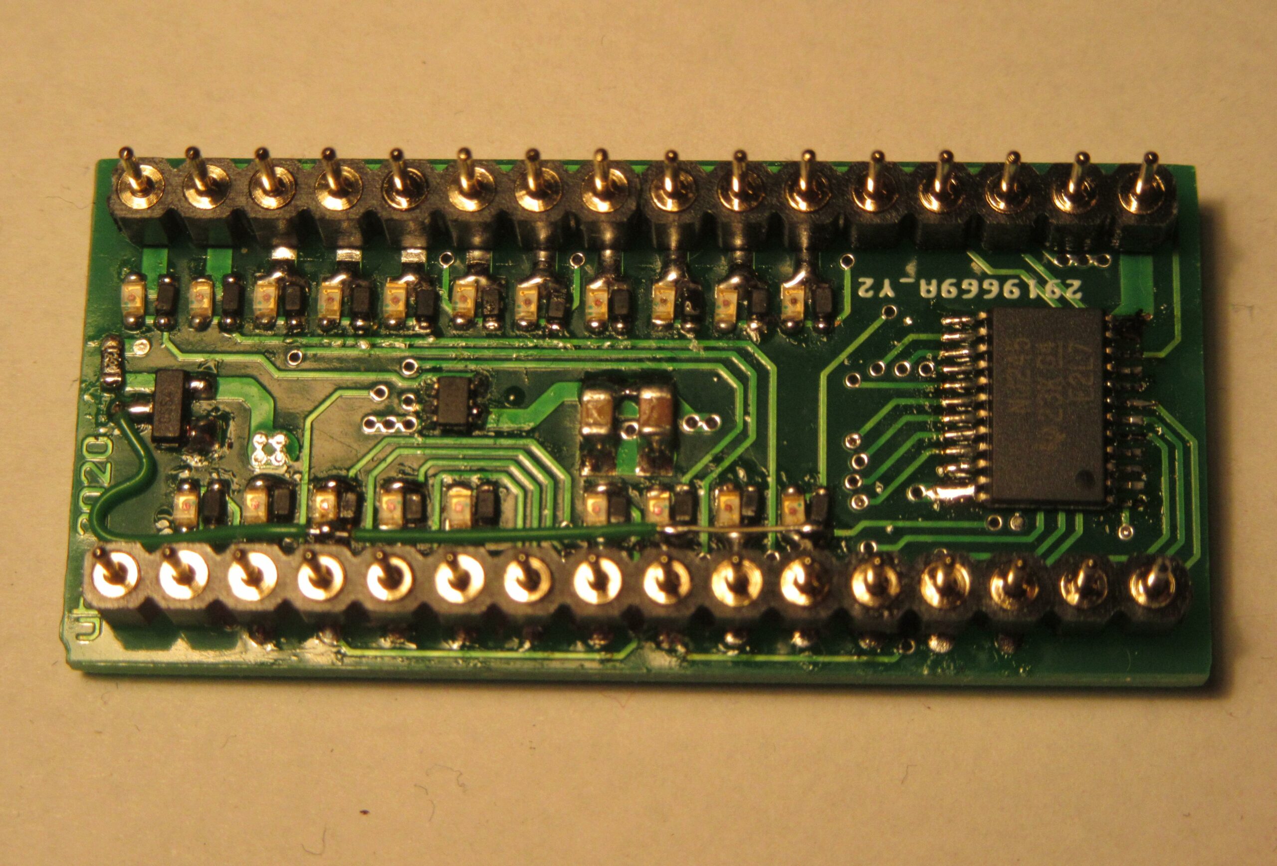
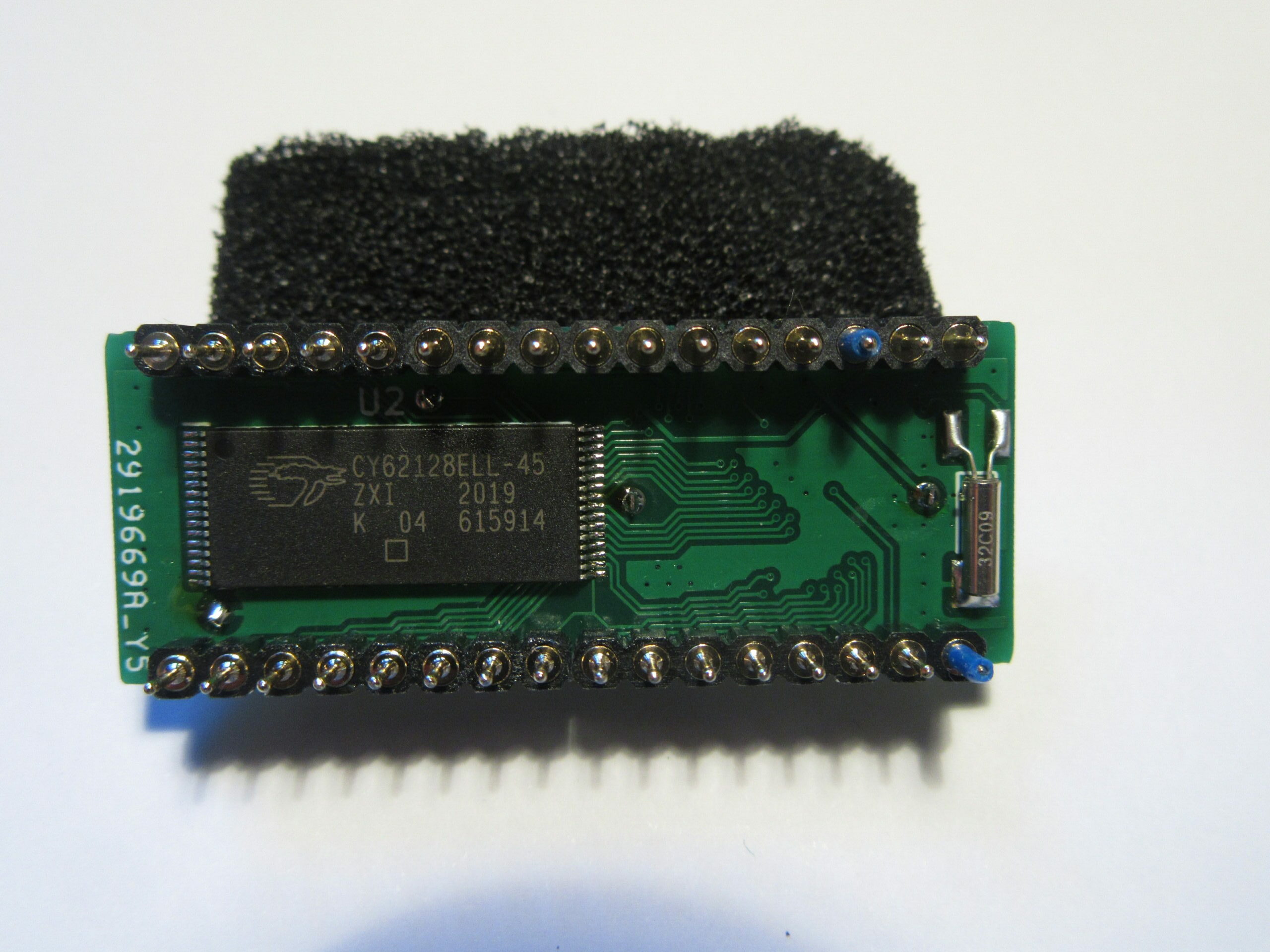
DS1650Y
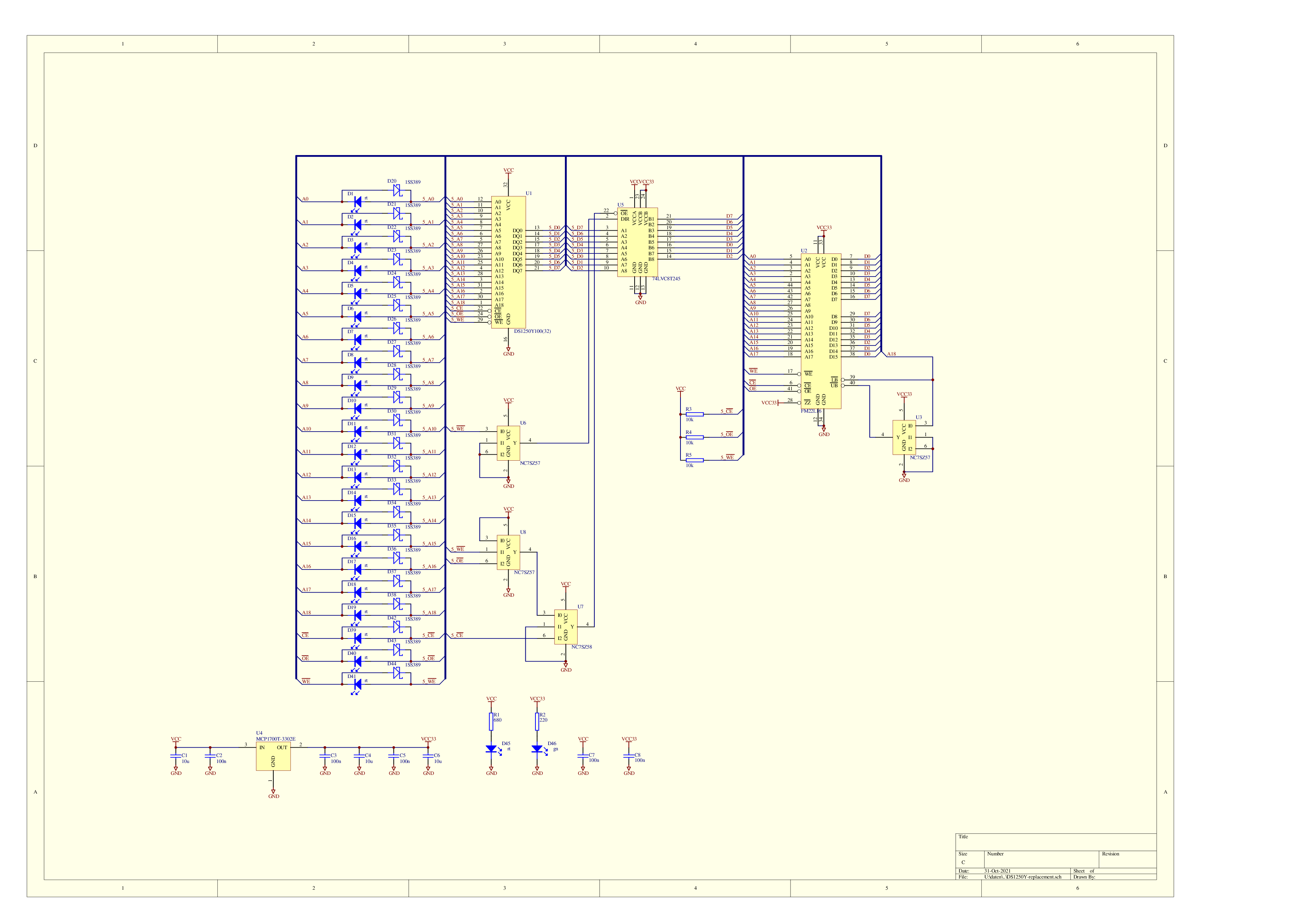
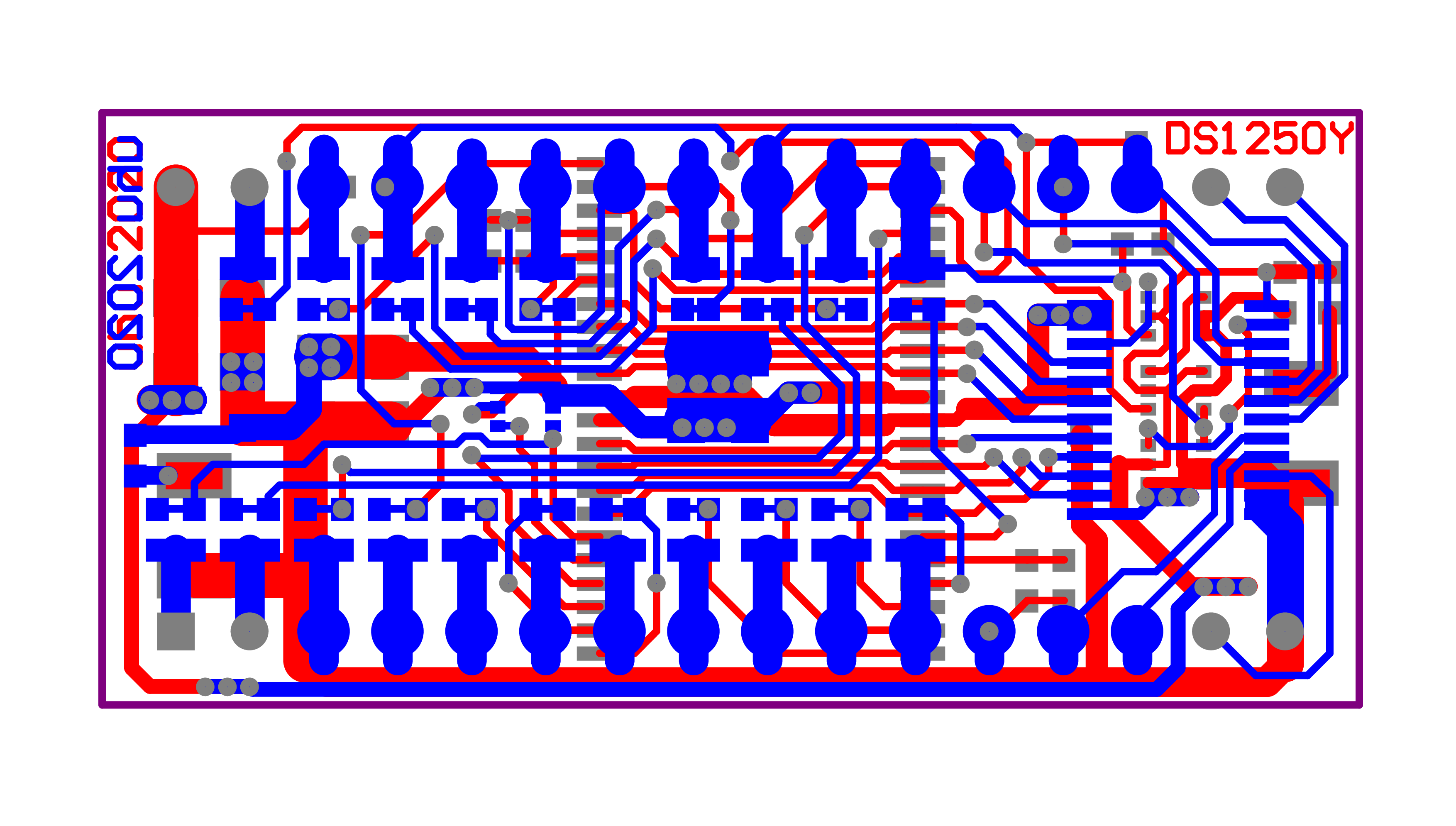
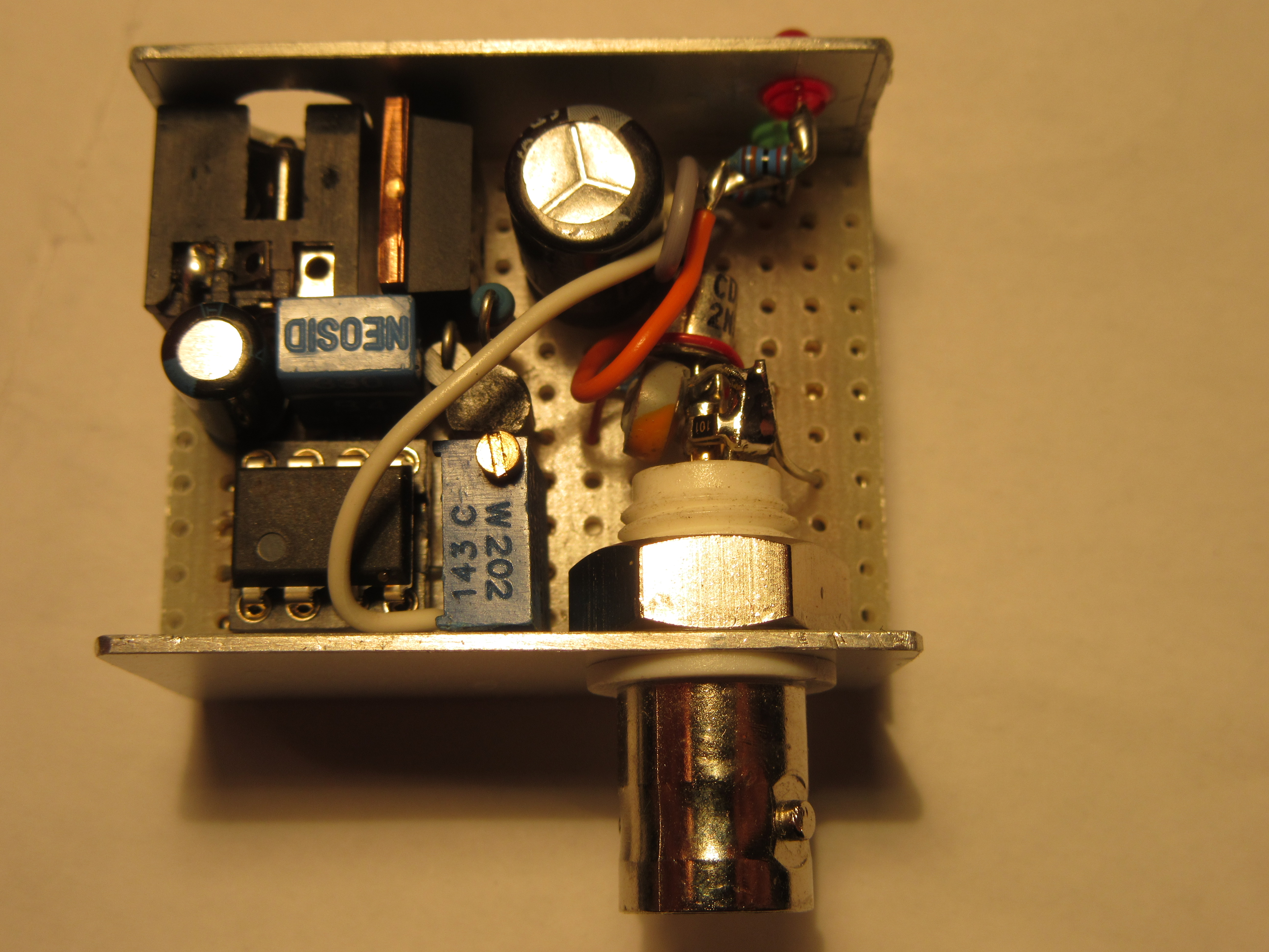
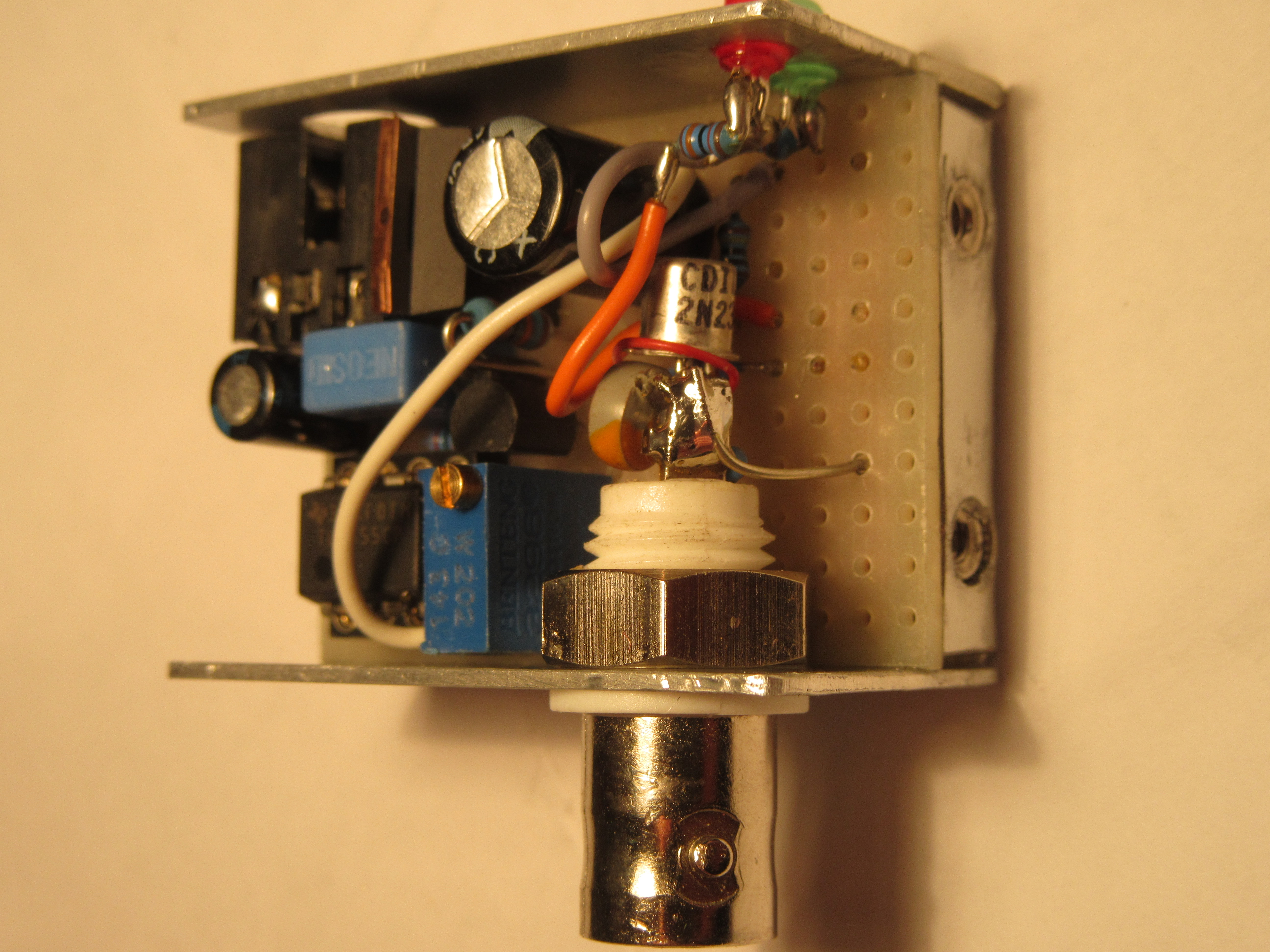
The replacement based on a FRAM for the 4MBit NVRAM DS1650Y I developed myself at the beginning of this year. It is described in detail in the article. In the TDS754C a DS1650Y is installed, but the write protection feature of the component is not used. The replacement with the FRAM module is therefore possible.
Installation
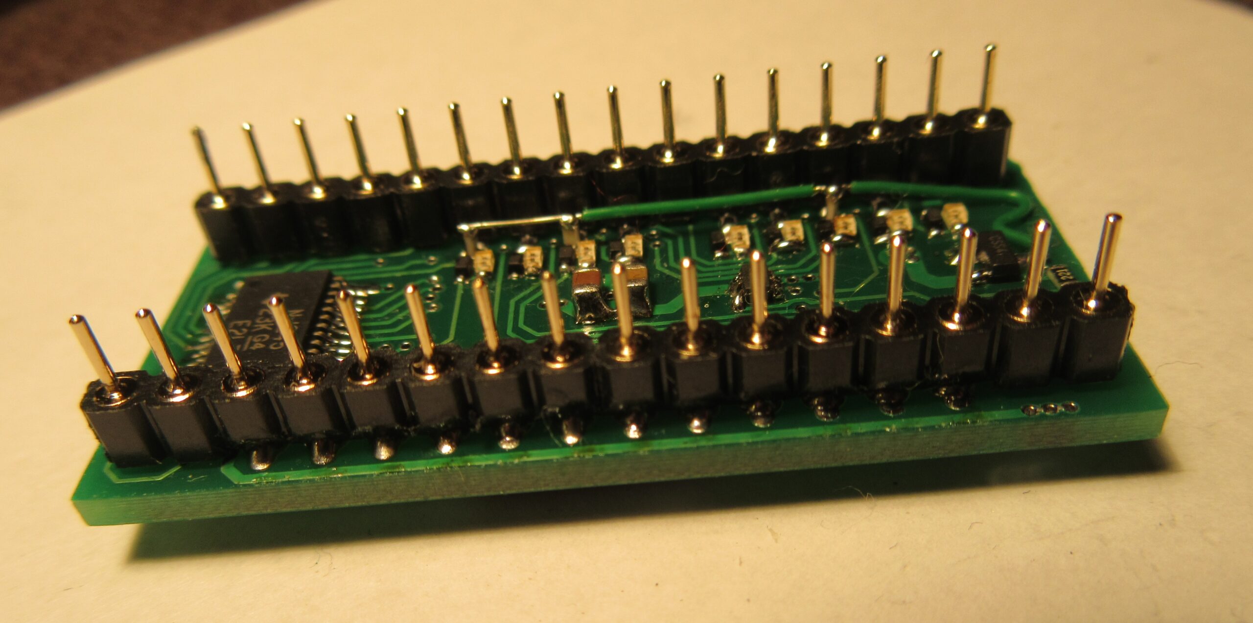
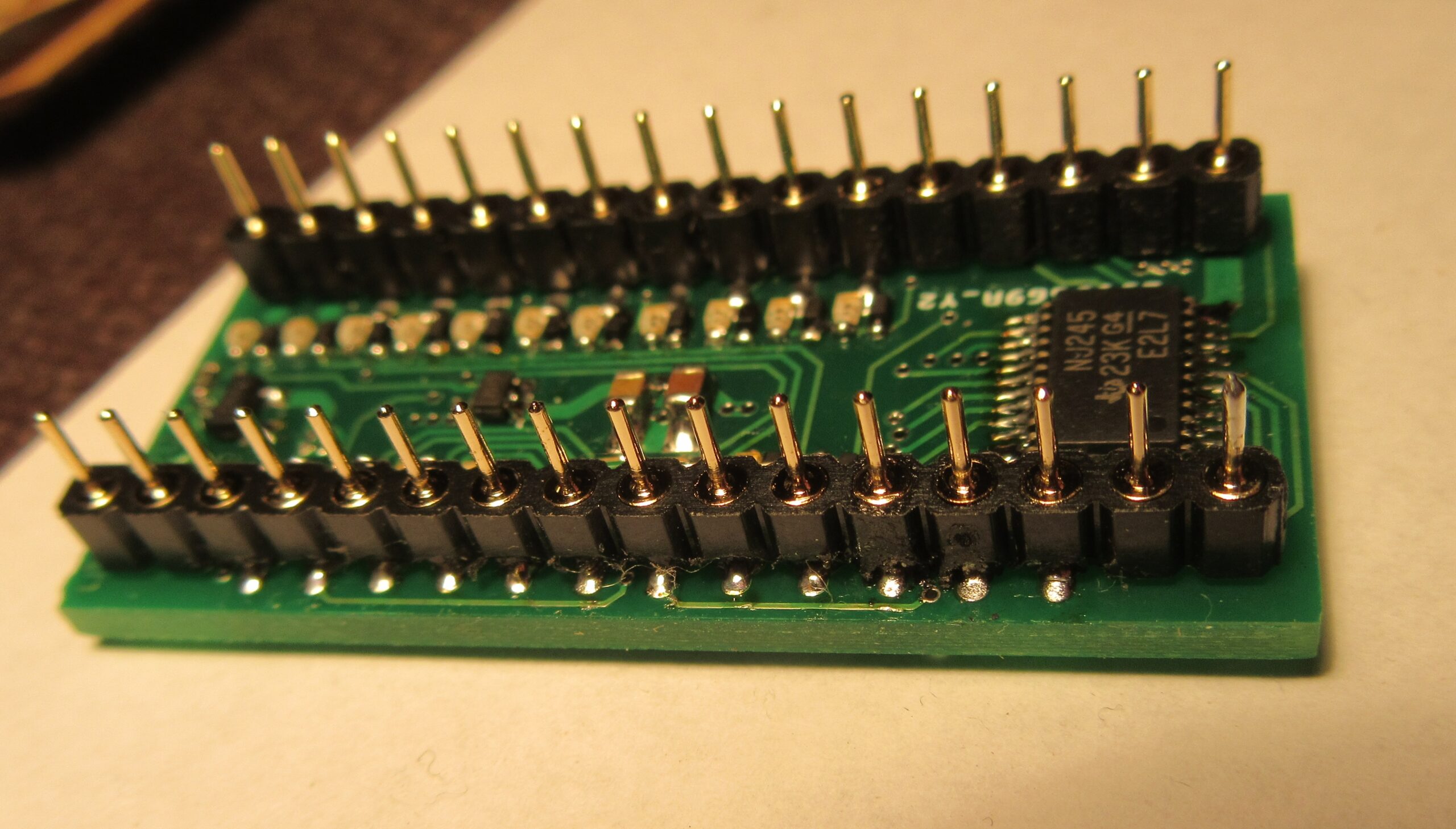
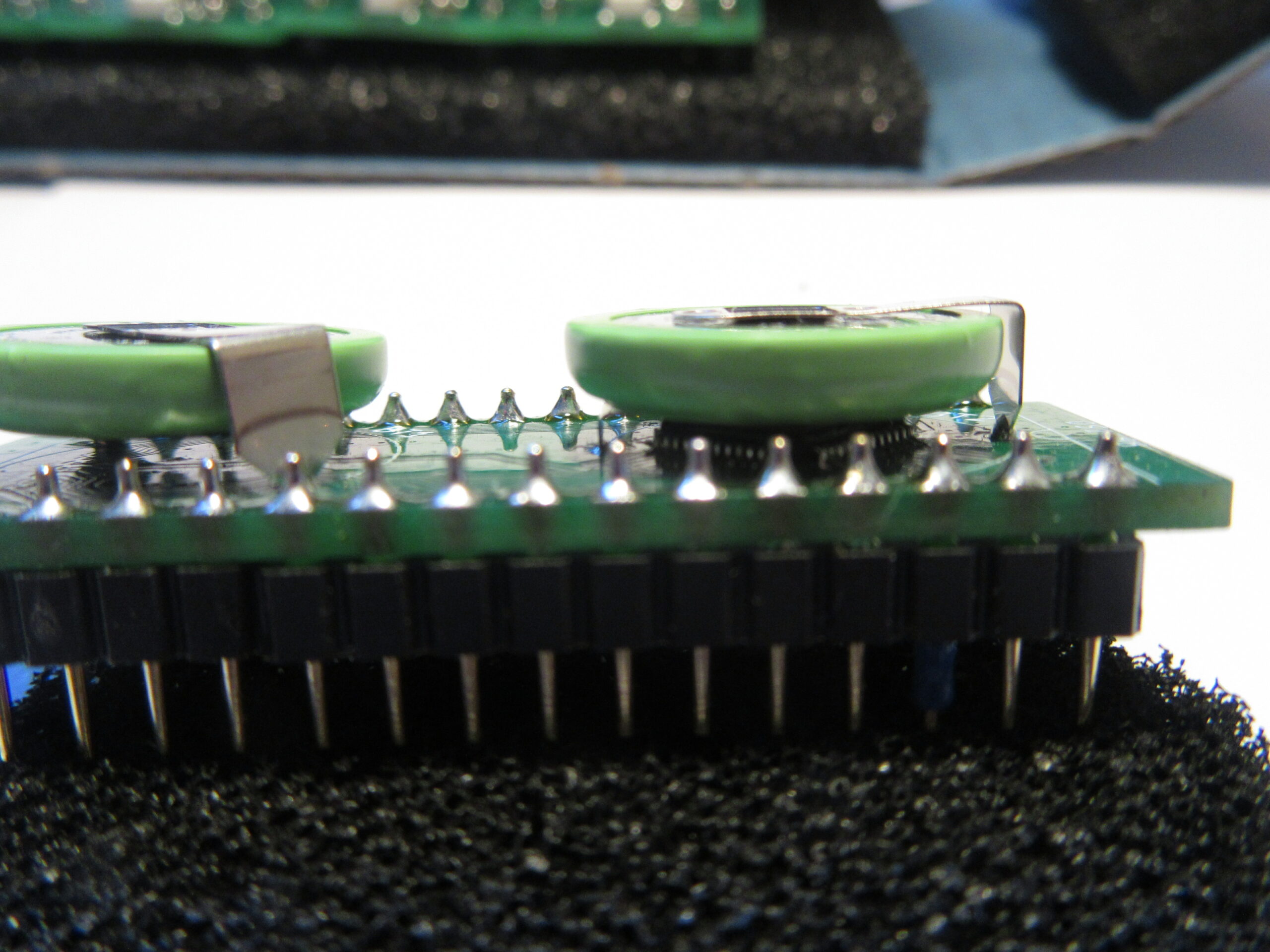
The new components are conveniently socketed. This makes it easy to remove the modules to replace the batteries, for example. Besides, it was uncertain whether the exchange would work. In case of problems, I could have simply put the two soldered out parts back into the socket.
As sockets I use some with a low profile. The contacts are partially recessed in the board. This makes the replacement part with socket only slightly higher than the original.
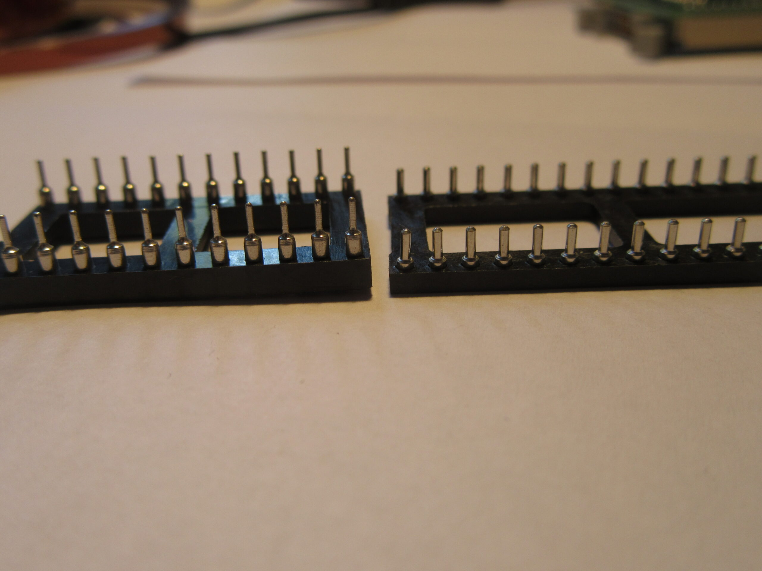
The two sockets were quickly soldered in place. It was annoying that the pin headers of the two replacement modules were a bit too thick. Thus they do not fit completely into the socket and are relatively difficult to insert and remove. I should have read the data sheets of the mechanical components beforehand.
Putting into operation
First, the device reported an NVRAM CRC error after power-on. Maybe the memory was written during the backup which leads to an invalid checksum. The attempt to restore the backup with the above linked “tdsNvramFloppyTools” was successful. The device now starts again as usual and at least the two replaced parts will do their job for many more years.