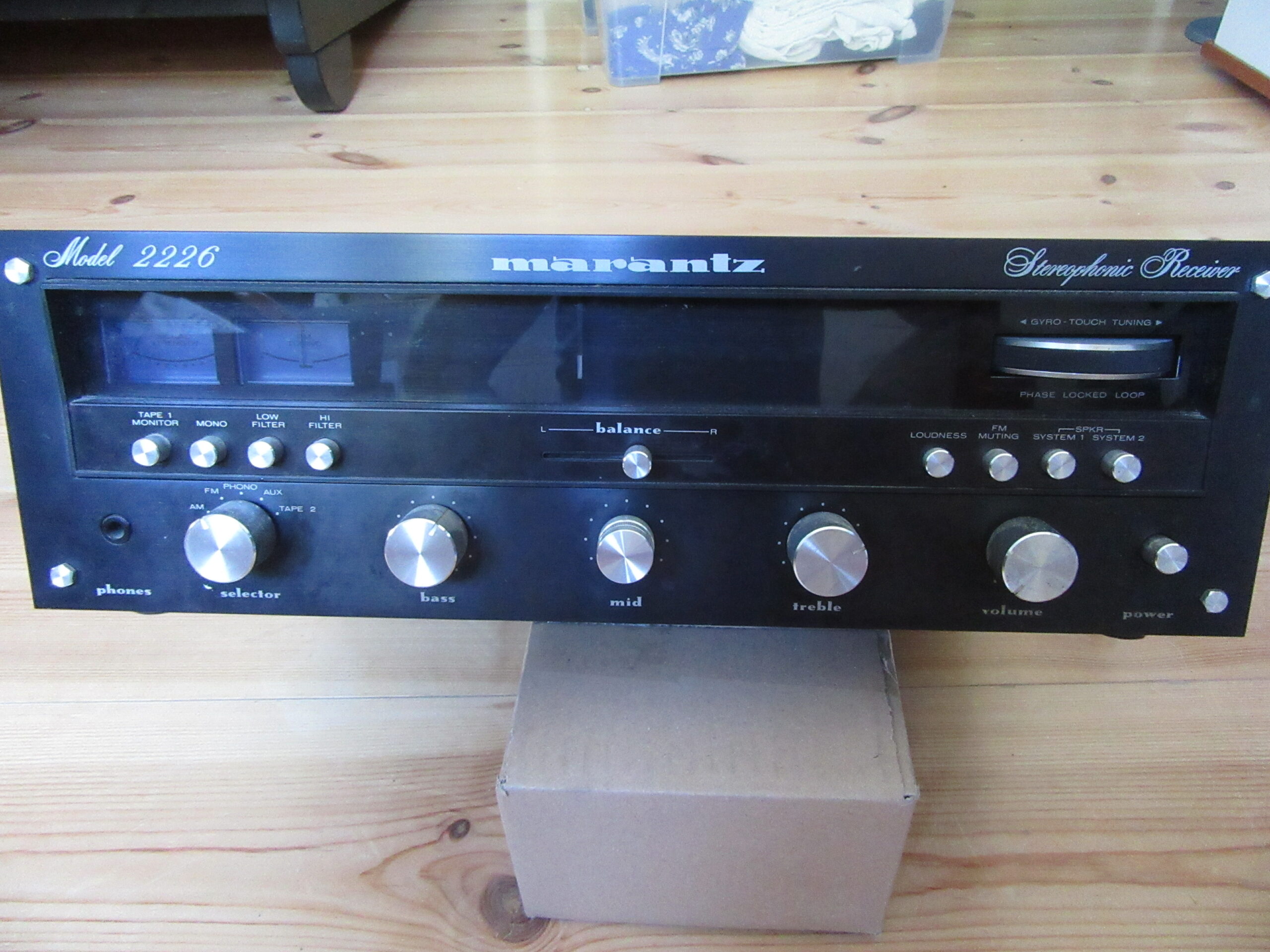
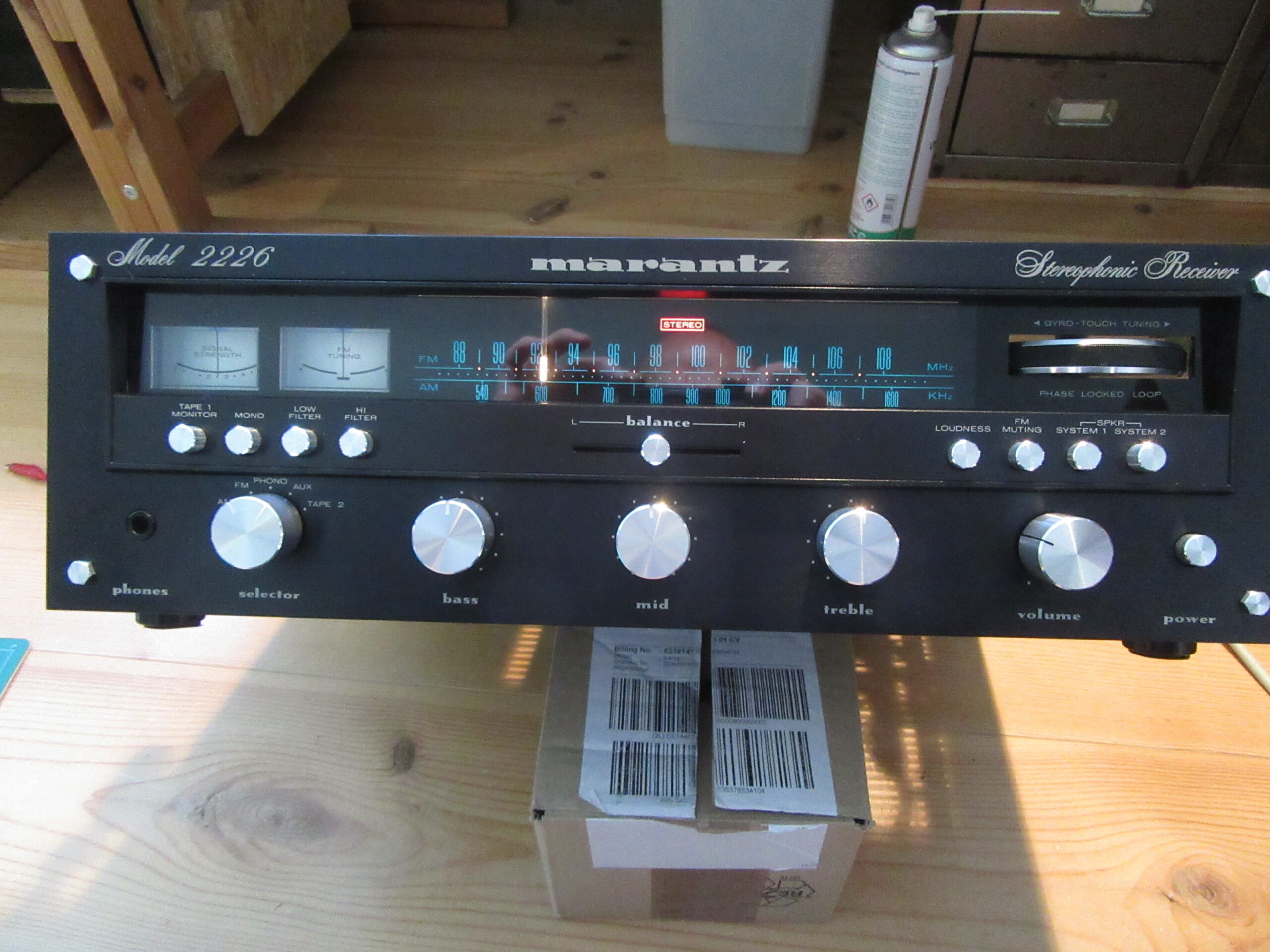
The unit was in excellent condition after 42 years of operation, so the restoration consisted mainly of a meticulous cleaning. Nevertheless, a few small things had to be fixed
one of the big knobs was no longer original
the dial illumination was defective
squeaking noises during tuning
broken off plastic corner at the scale holder
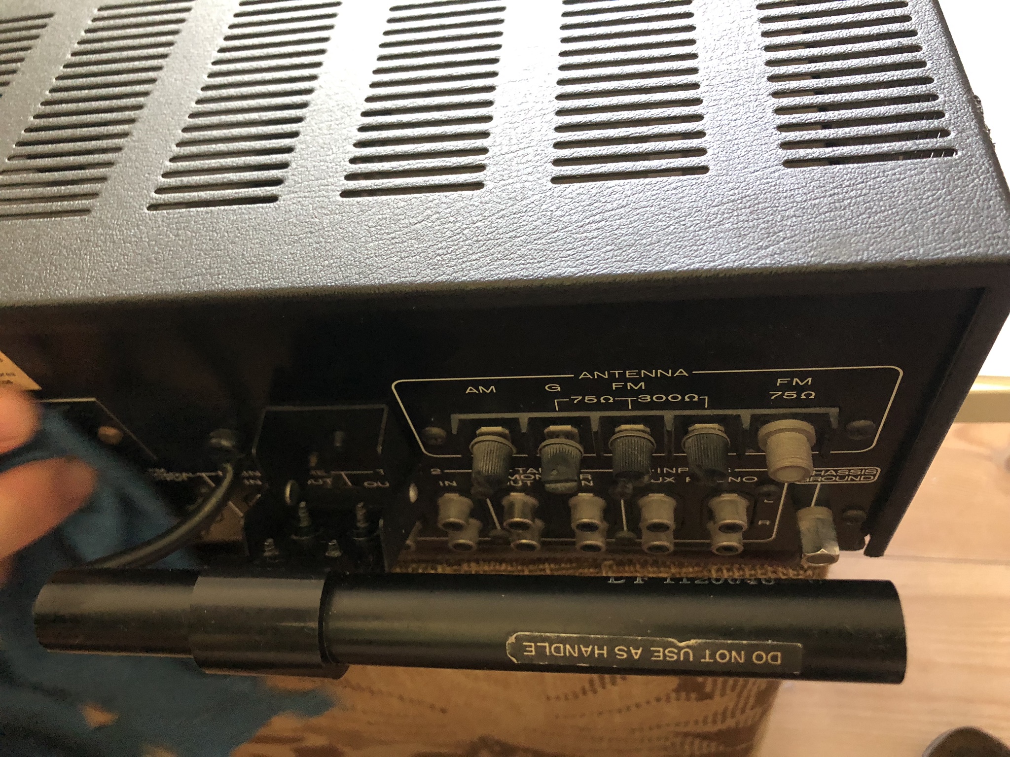
I found a new original knob on the internet for an outrageous 10 Euro or so. For the scale illumination I replaced the 6x30mm 8V pilot bulbs with 12V versions. This makes the illumination darker, but it lasts forever and the plastic parts are no longer stressed by heat. I also reversed the unconventional conversion to E10 bulbs. I got rid of the squeaking noises by using Ballistol on the idler pulleys. And the broken off plastic corner I glued back on with rather toxic Dichlormethane. The potentiometers had only a slight scratching, so nothing has been done here yet. That will be repaired in 30 years.
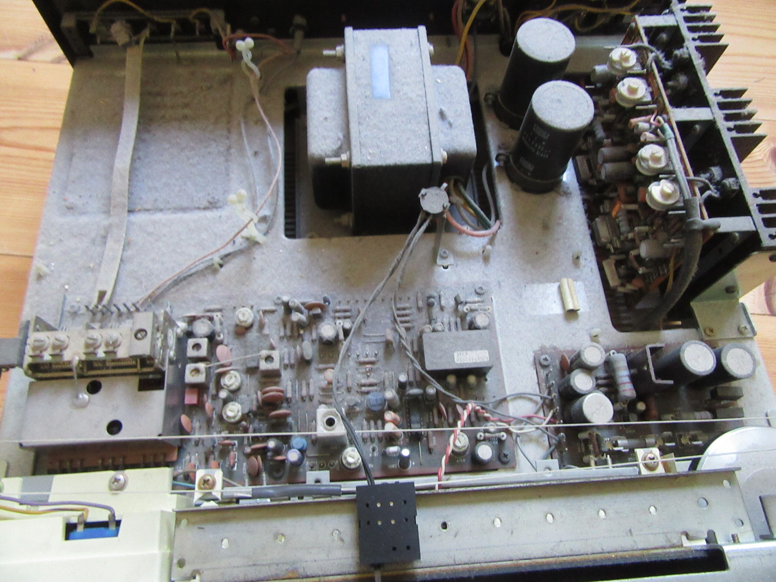
During cleaning I moved a 78XX voltage regulator with heat sink too much. This caused a hairline crack to form next to the solder joint and of course the receiver stopped running. But the fault was quickly found and fixed.
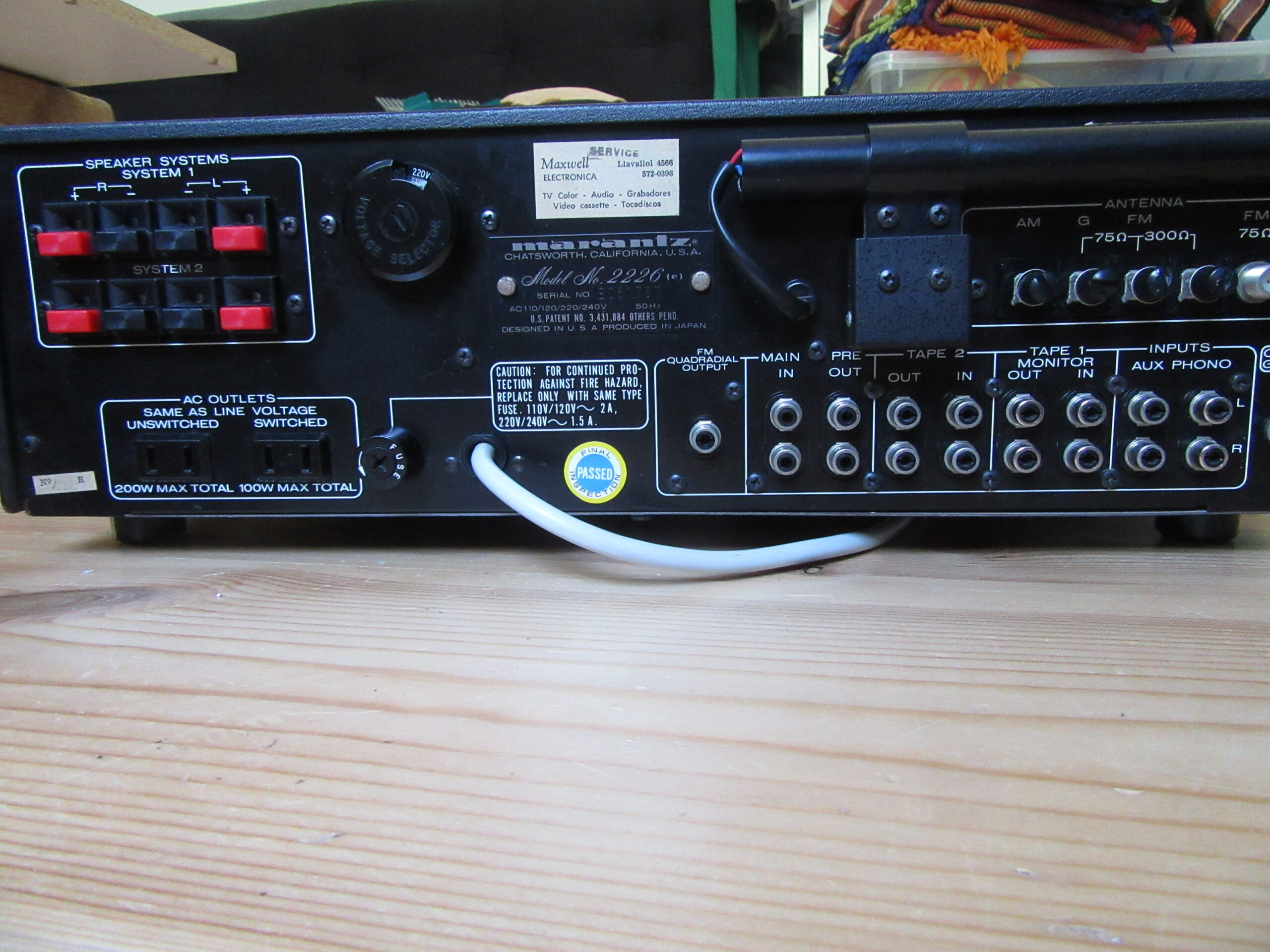
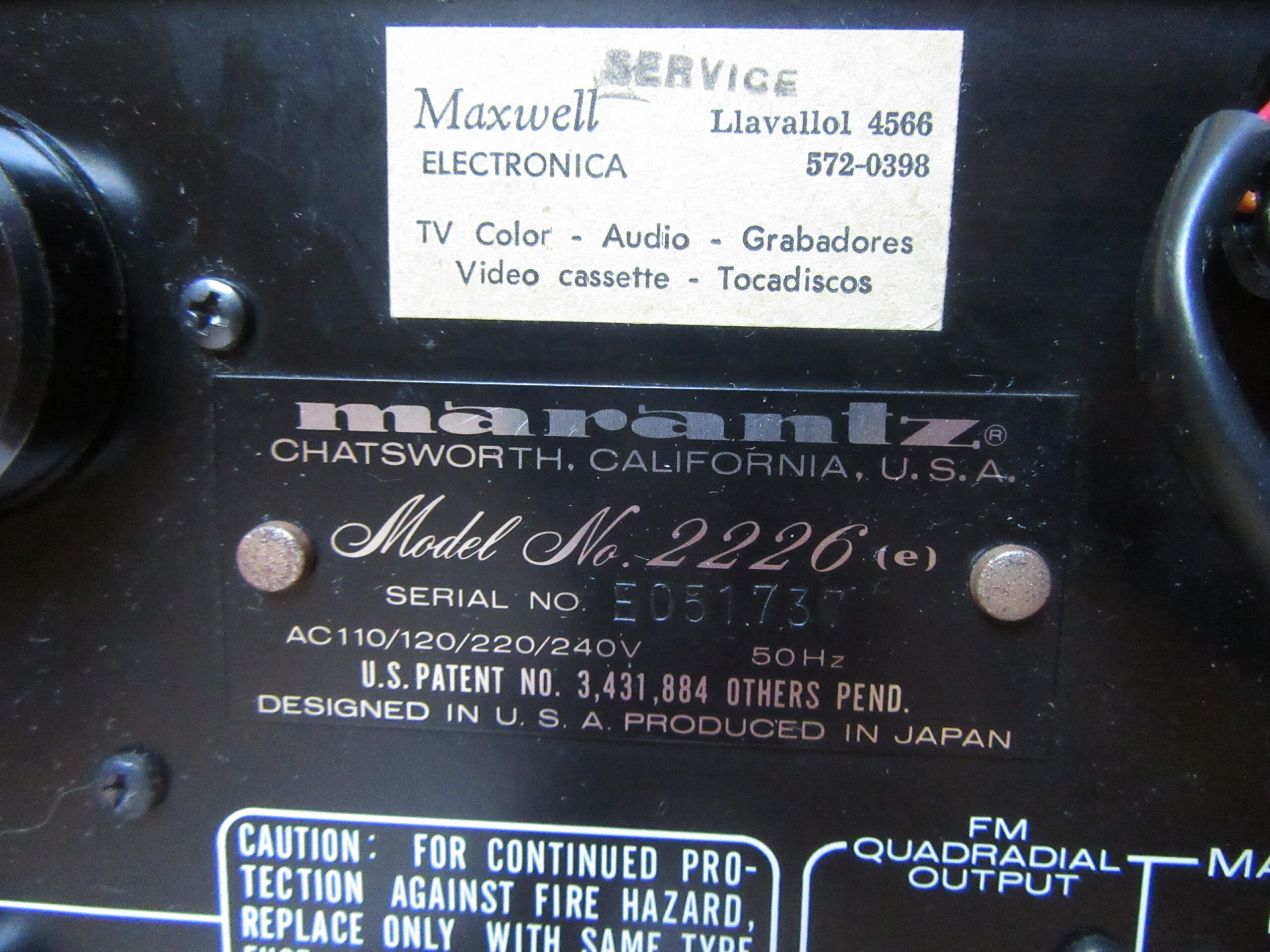
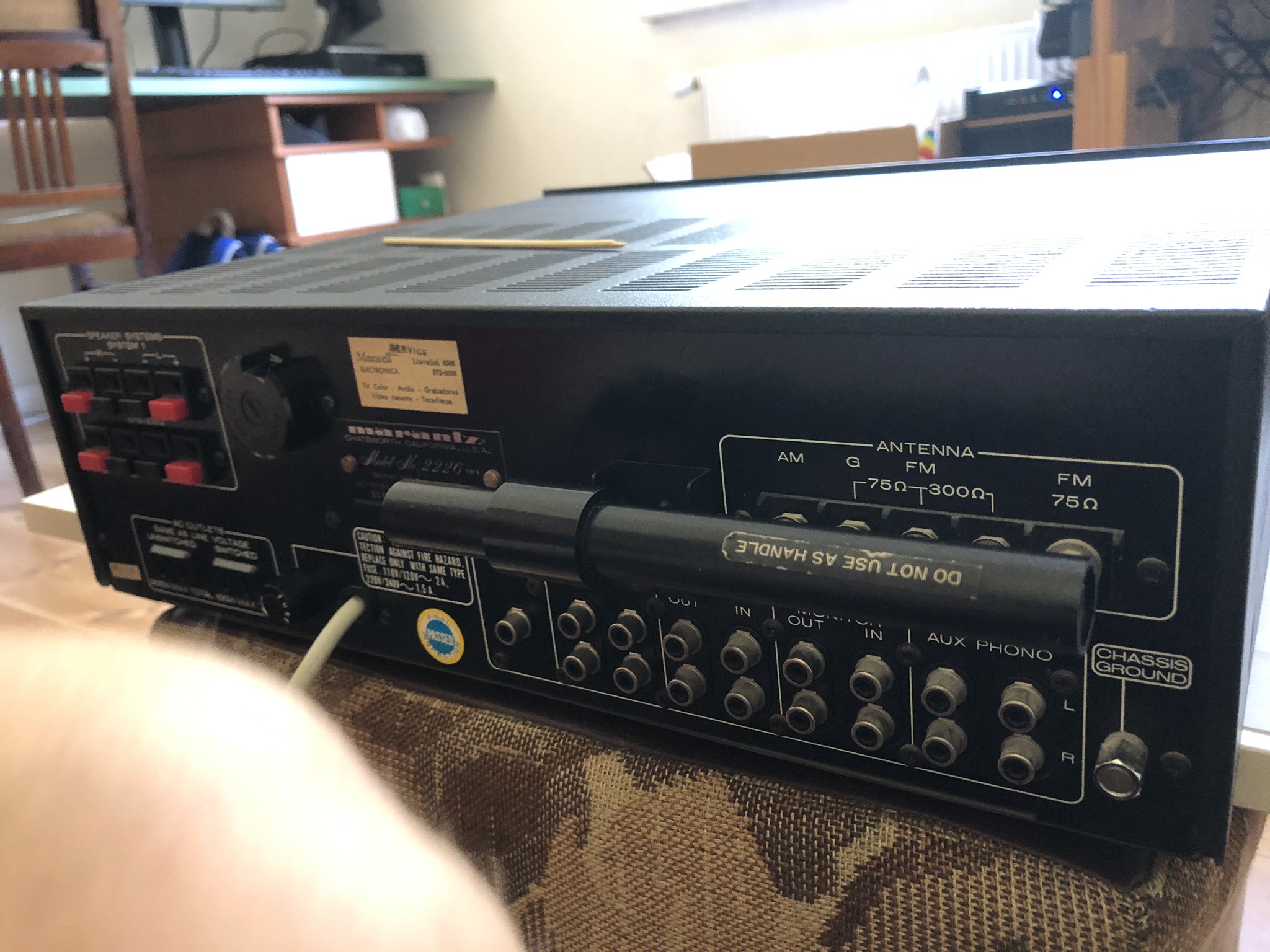
There was also a bit of family history involved, as the unit traveled with my girlfriend’s family to Buenos Aires in the late 70s. After a few years there and at least one repair, the receiver came back to Germany as part of the family. A sticker of the service workshop “Maxwell Electronica” still testifies to the stay in Argentina. At least Google Maps still finds the company at the given address.
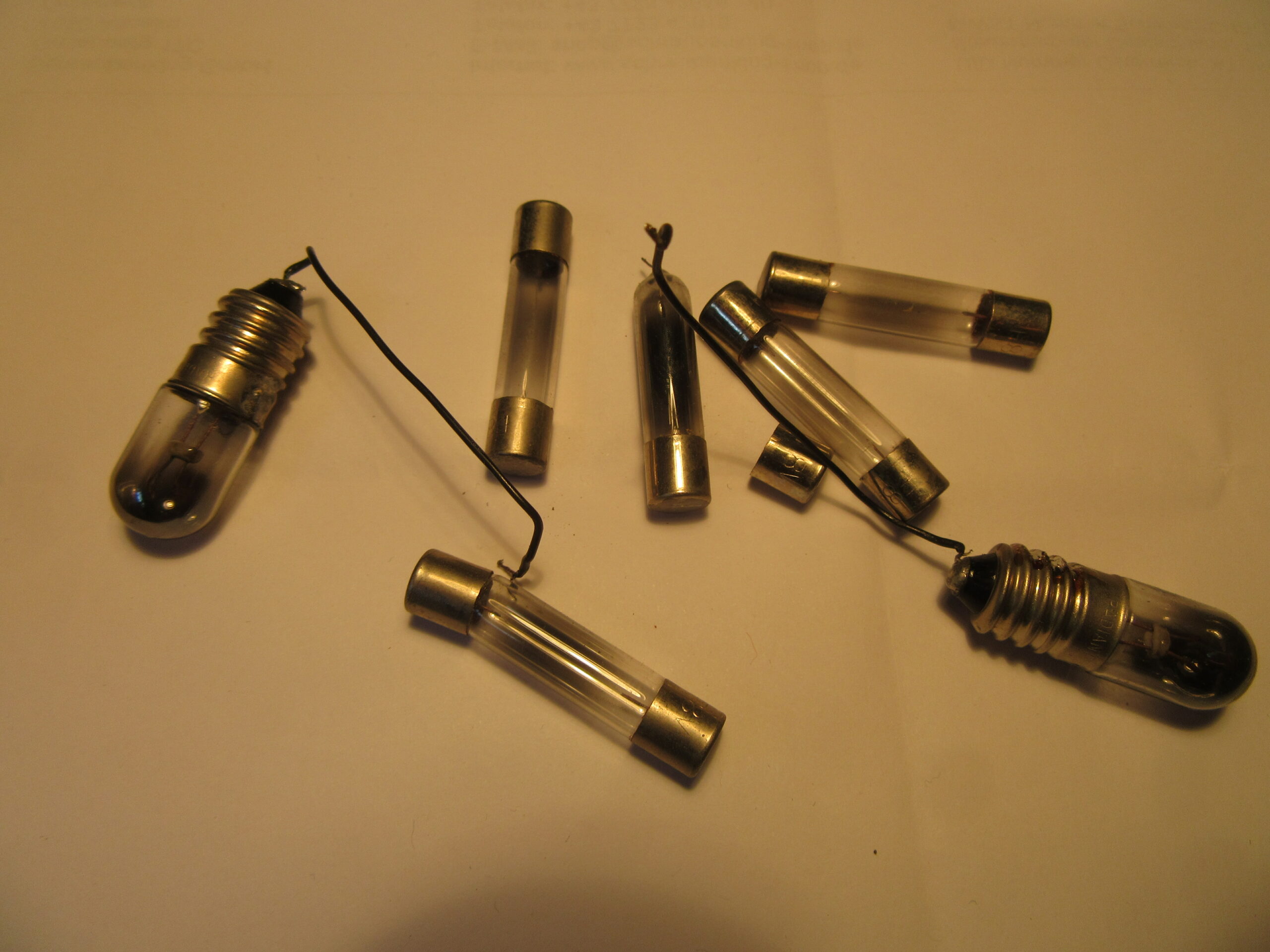
The workshop apparently repaired the scale lighting and adapted instead of the pilot bulbs incandescent lamps with E10 base. They had too much power and the plastic parts got too warm. Fortunately, the resulting discoloration can only be seen from behind.
But now the photos, without comment. First the initial state and part two with pictures after the repair.
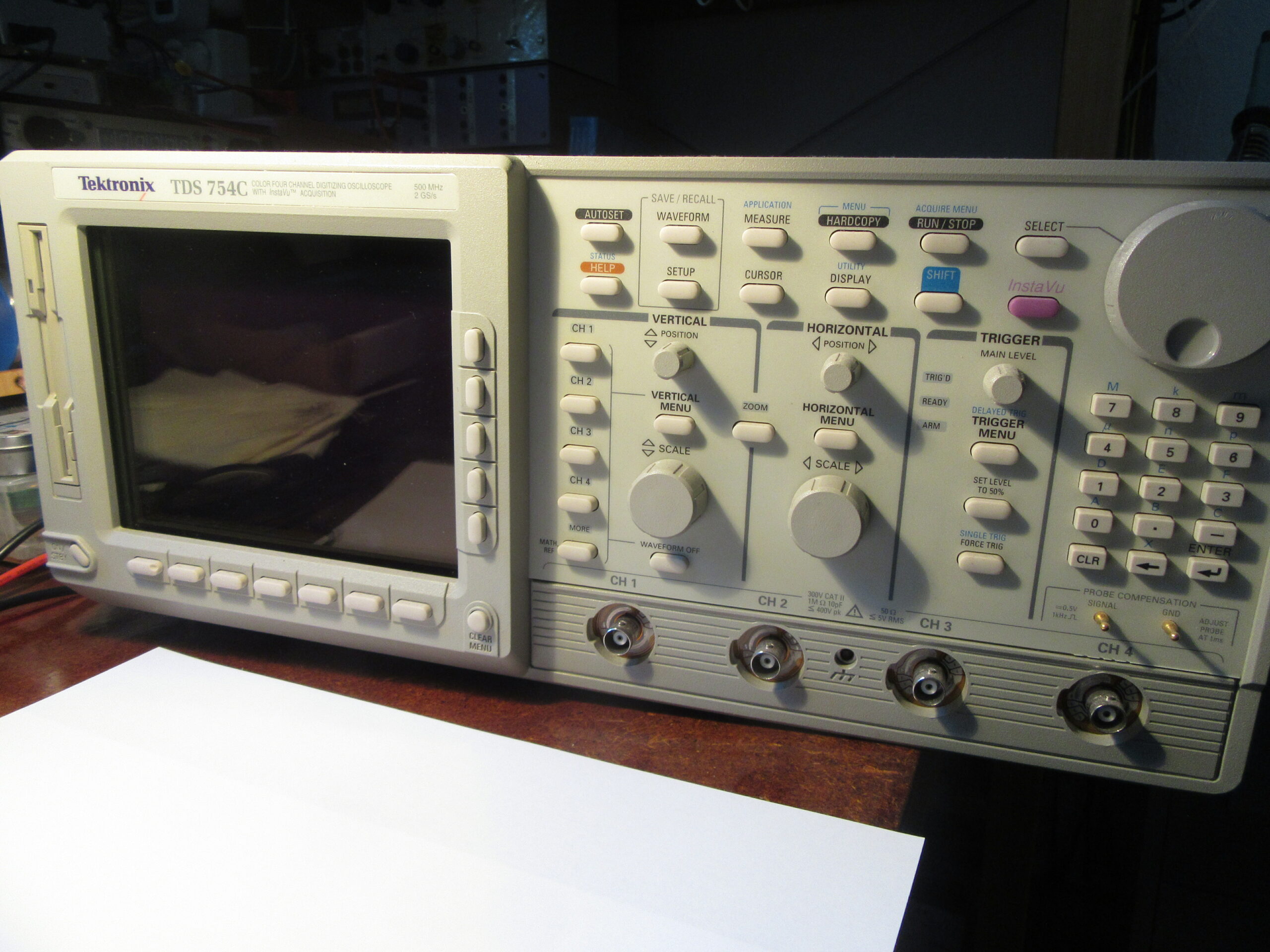
Finally there was a day off at the weekend. This time I wanted to use it to perform a maintenance on my Tektronix TDS754C digital oscilloscope that had been pending for years. The plan was to replace the two ICs from “Dallas Semiconductor” with integrated lithium battery. And that before they fail and lose all data. After 24 years. There is no more time to waste.
TDS754C Front view
Preparation
The preparation for this maintenance started years ago and took a long time, as it is with hobbies. Two things I had to do in advance:
Upgrade my homebrew programmer to 4MBit and make it able to read and write FRAM and NVRAM chip types.
Building a replacement for DS1250Y or DS1650Y chips.
I had already finished the extension of my programmer in 2018. I was able to check off the second item this spring and have described it in detail here.
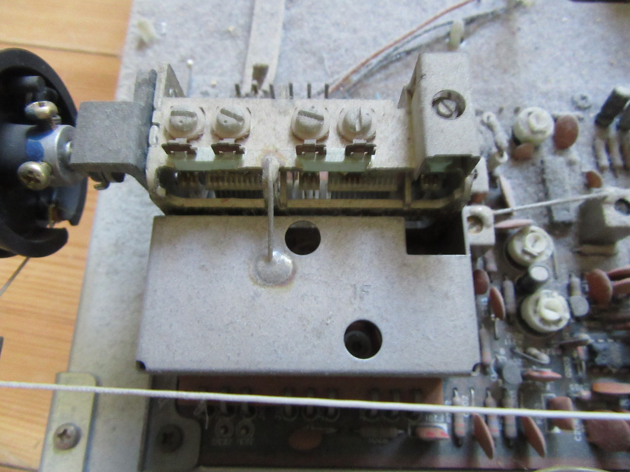
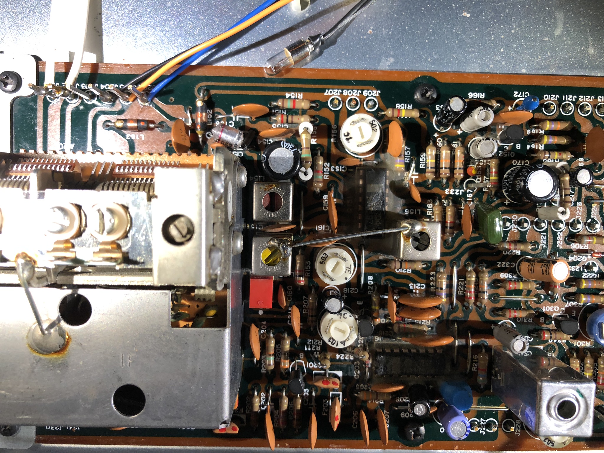
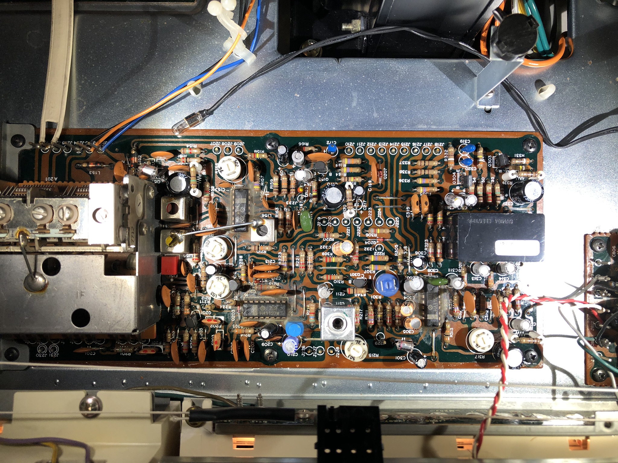
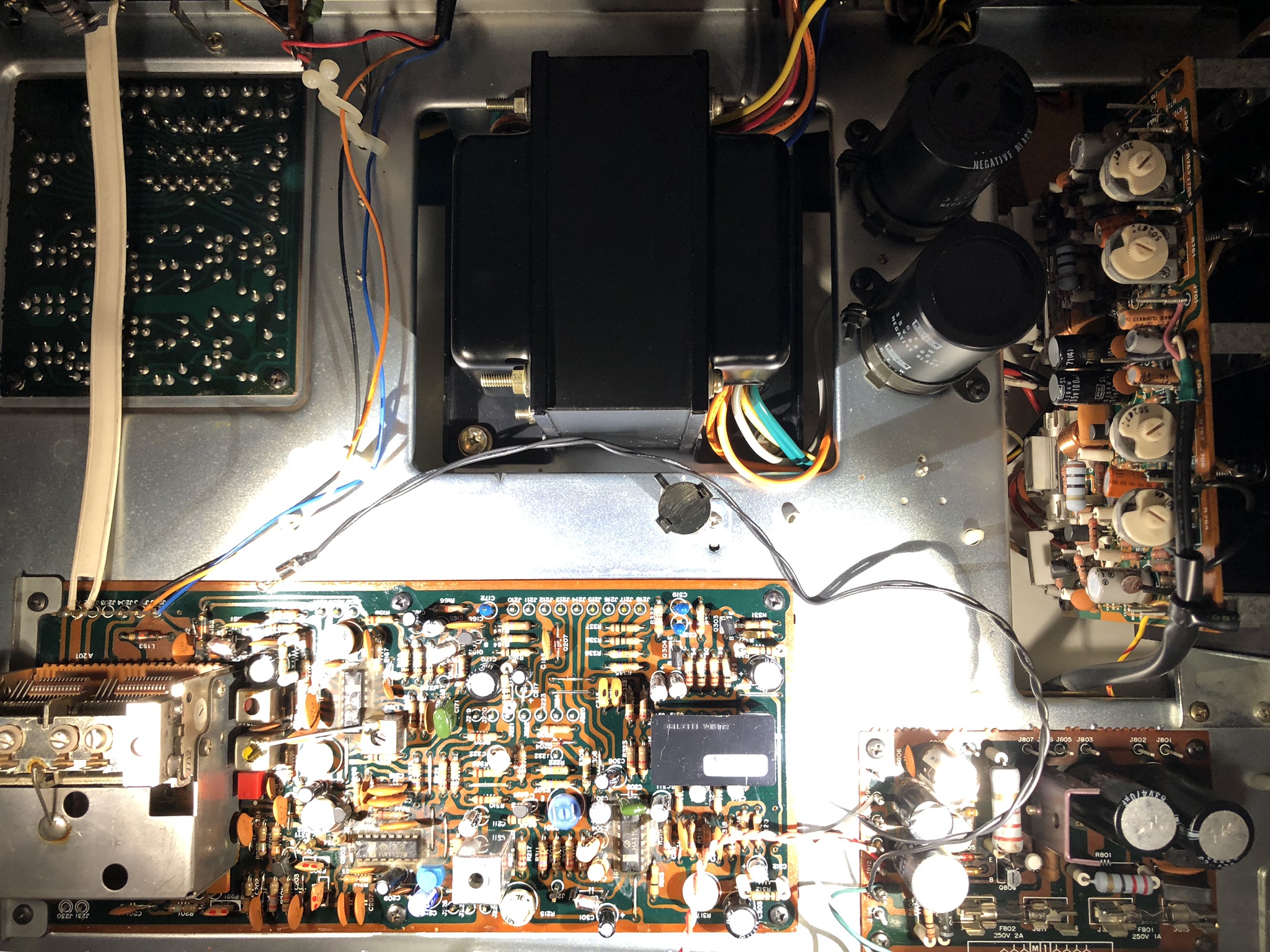
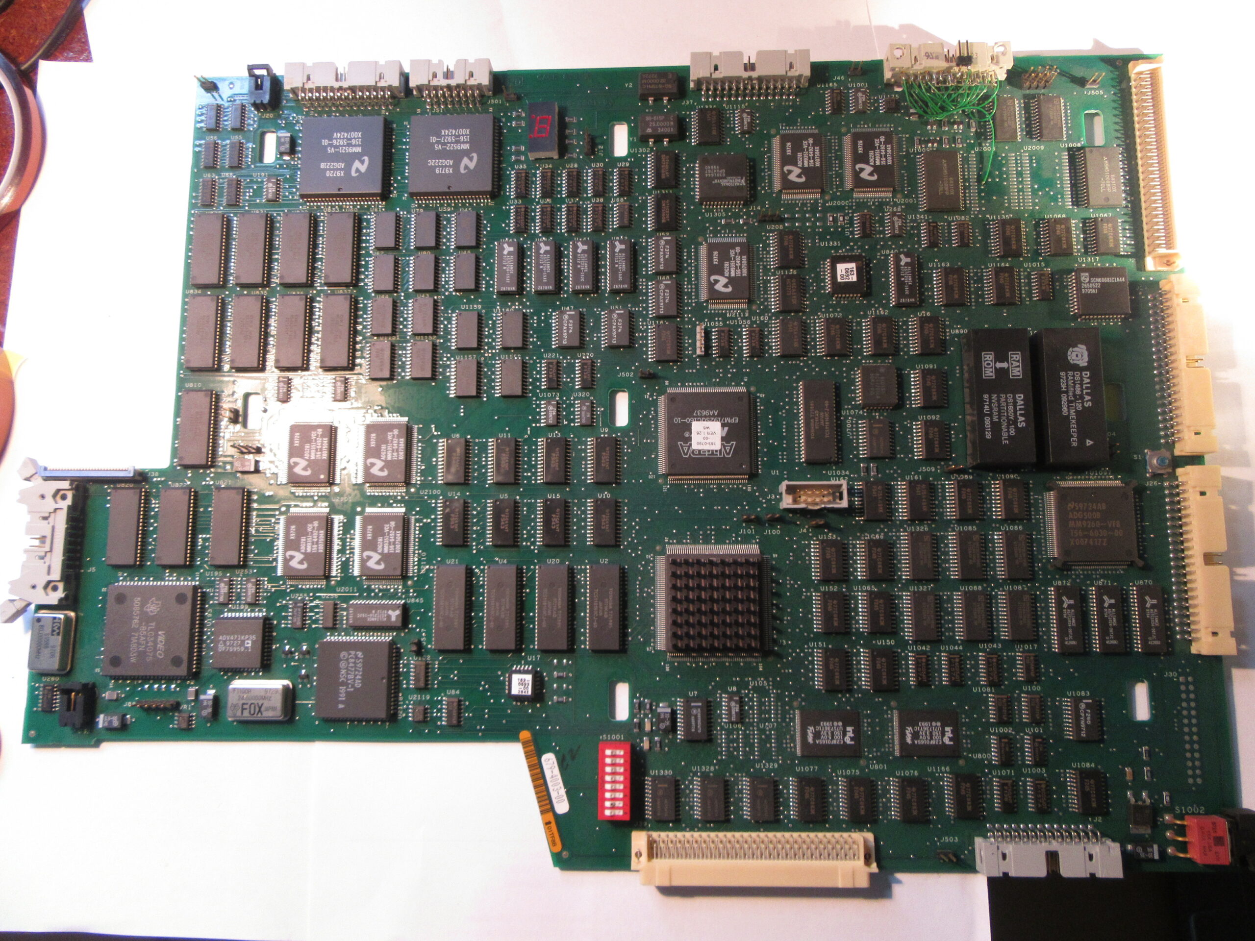
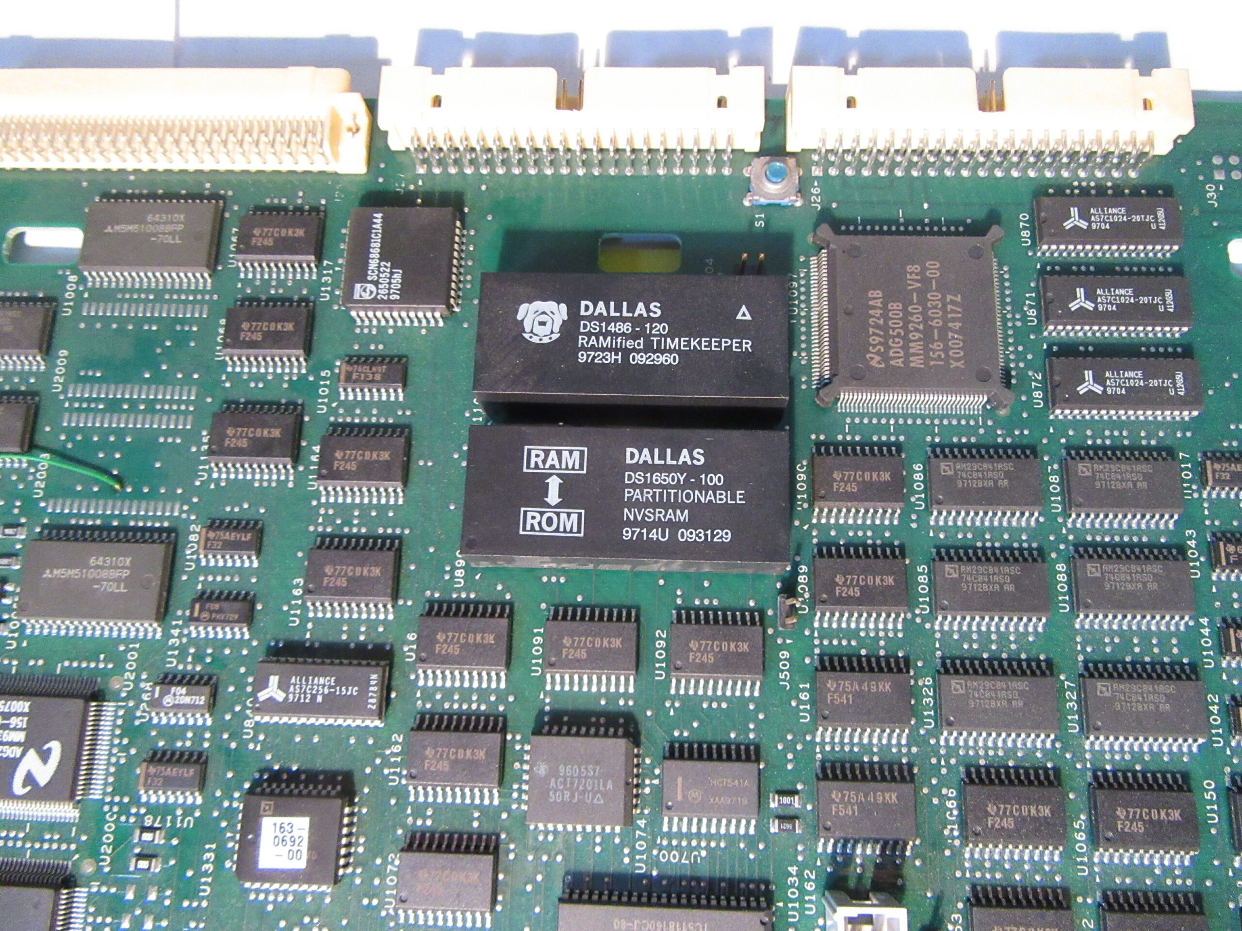
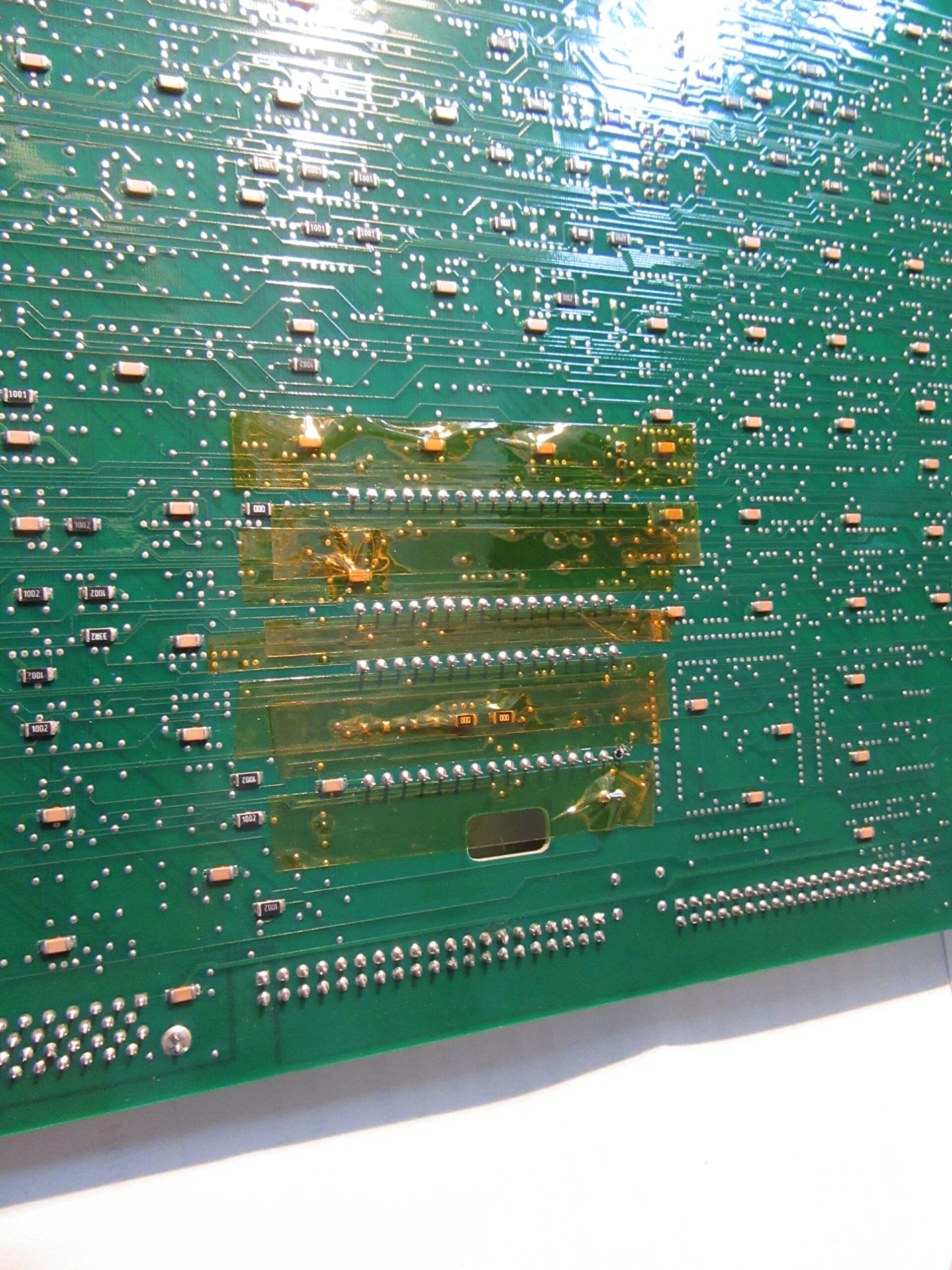
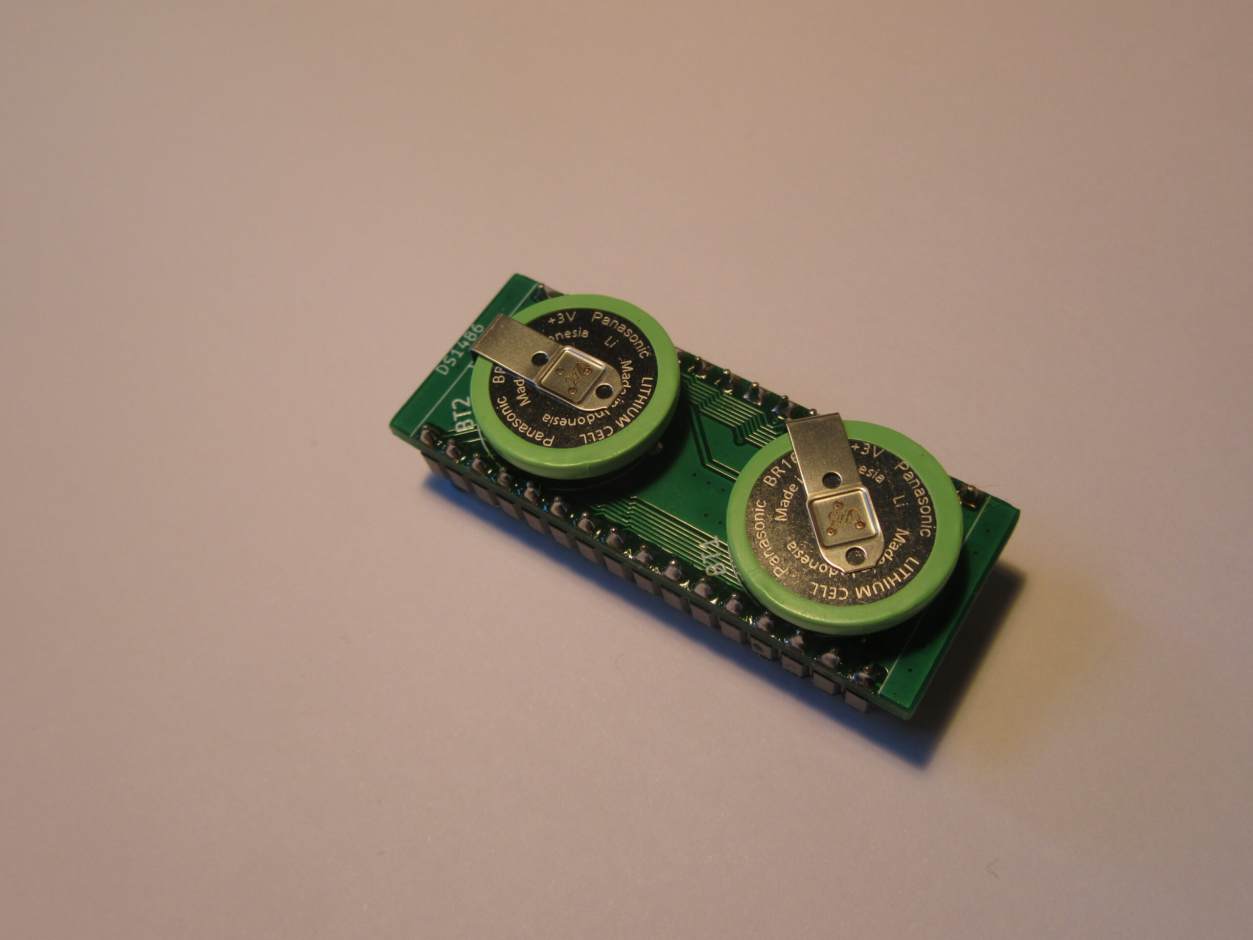
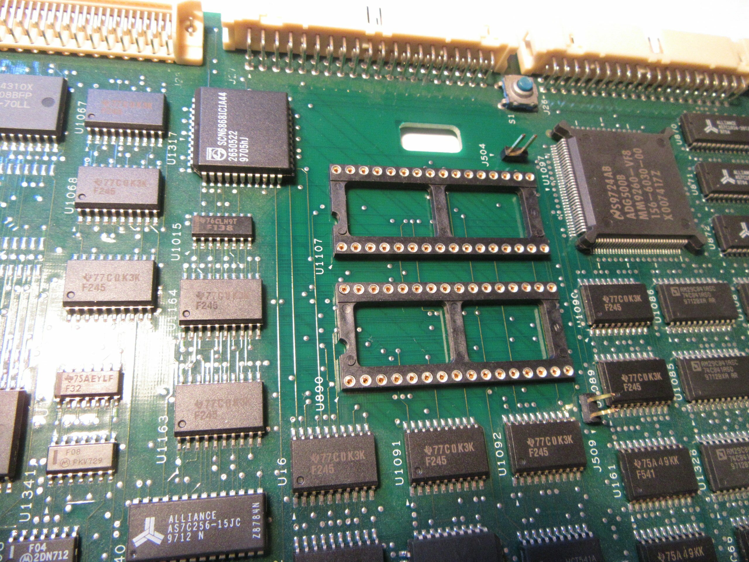
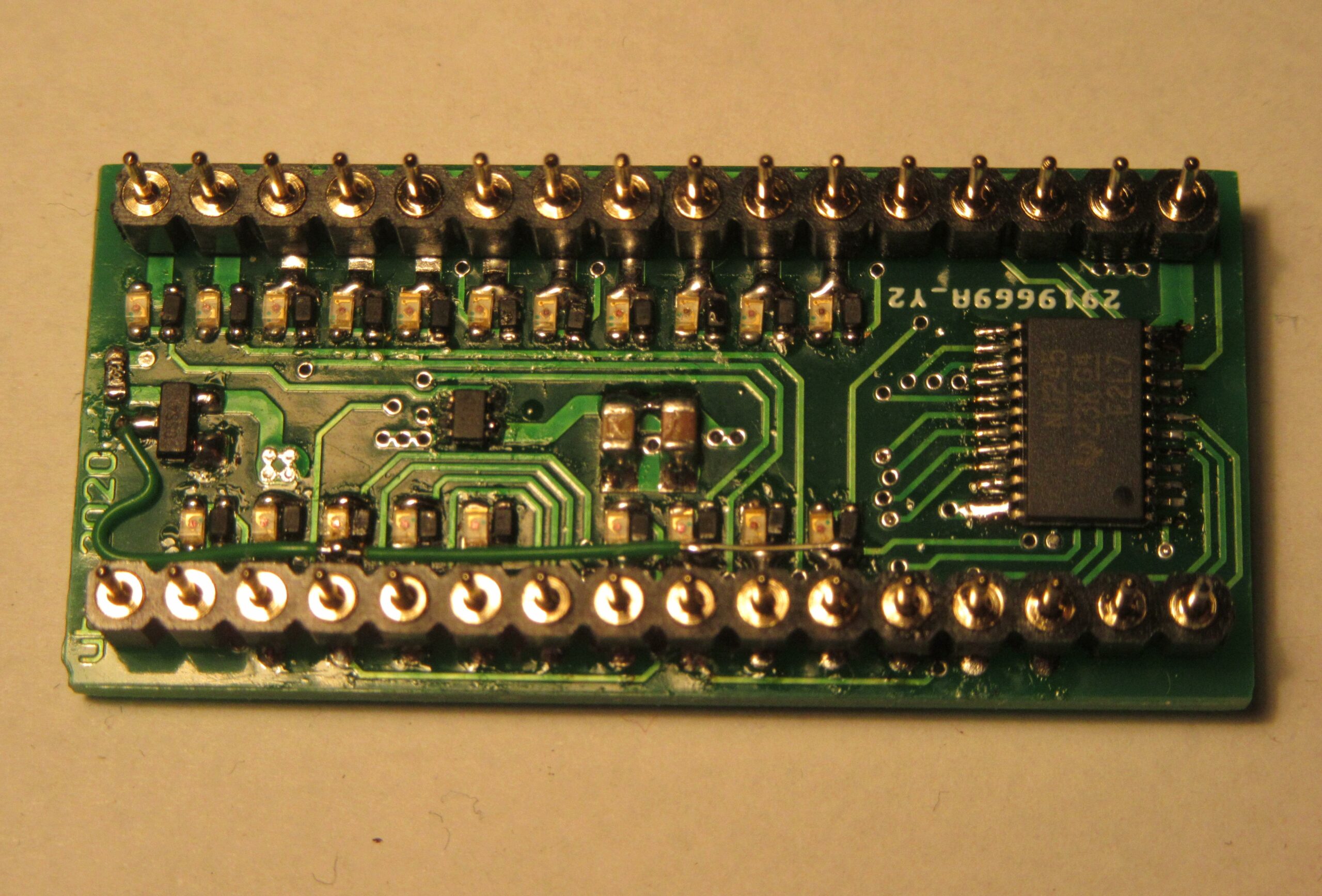
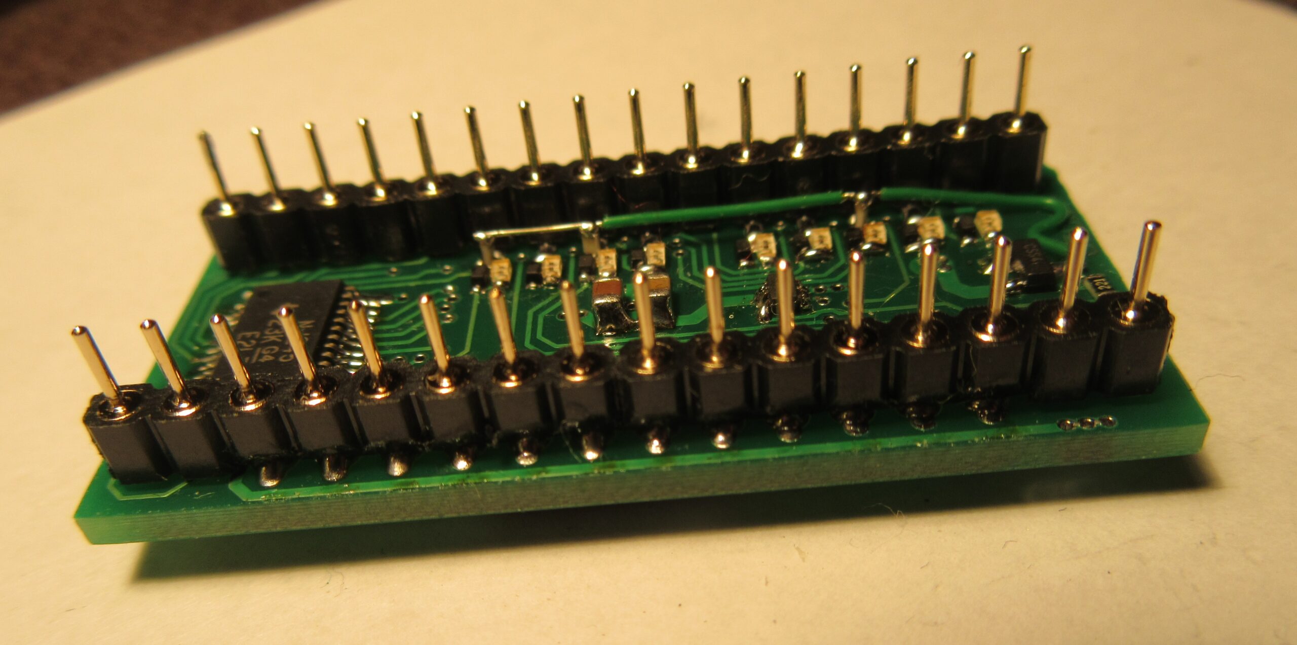
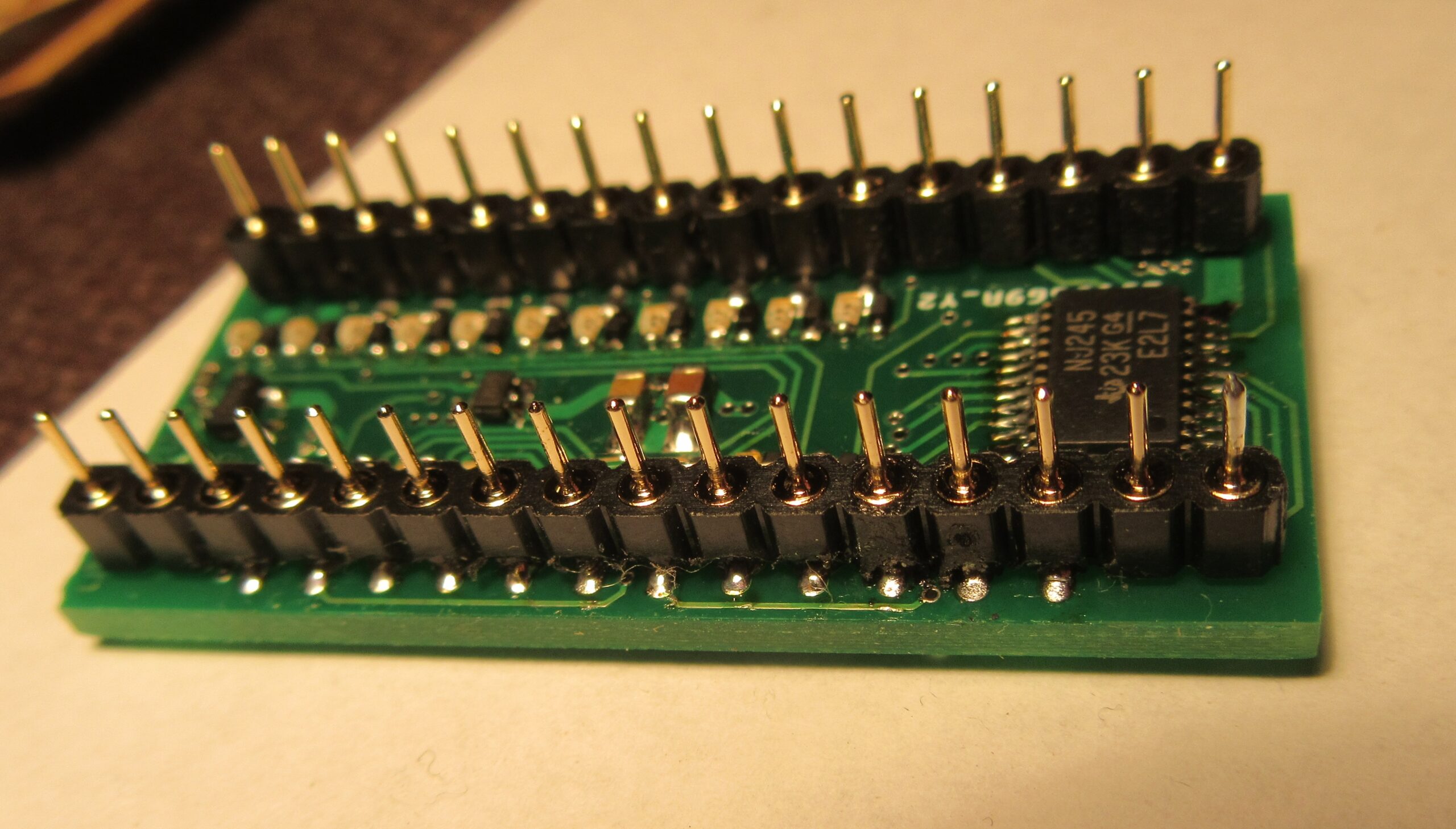
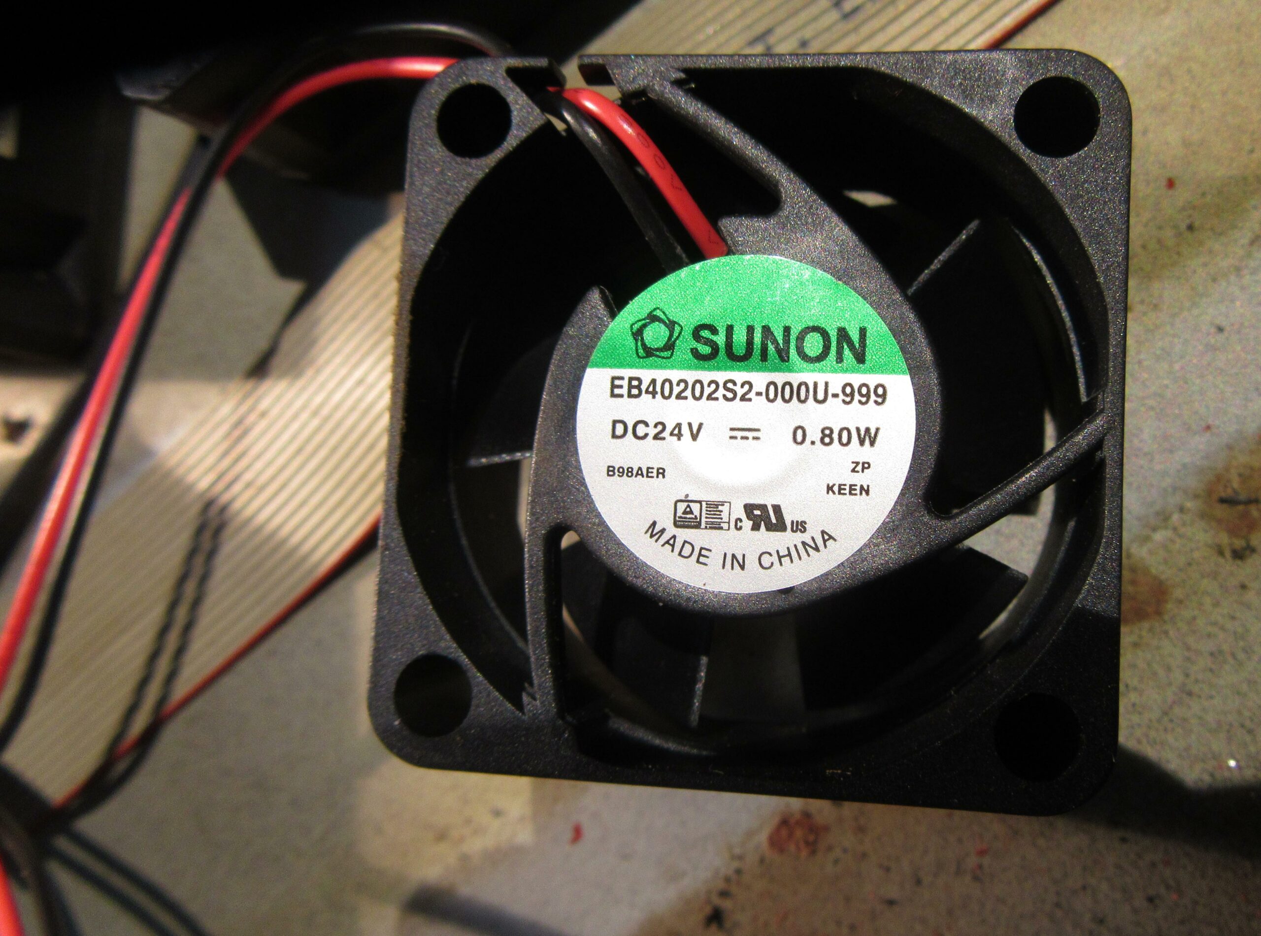
There are two of these ticking time bombs installed in the device, Dallas chips with integrated Lithium battery. I also described the problem with these components in more detail in this article. Specifically, it is a DS1486 RTC+1MBit NVRAM and a DS1650Y 4MBit NVRAM, both of which are soldered onto the CPU board.
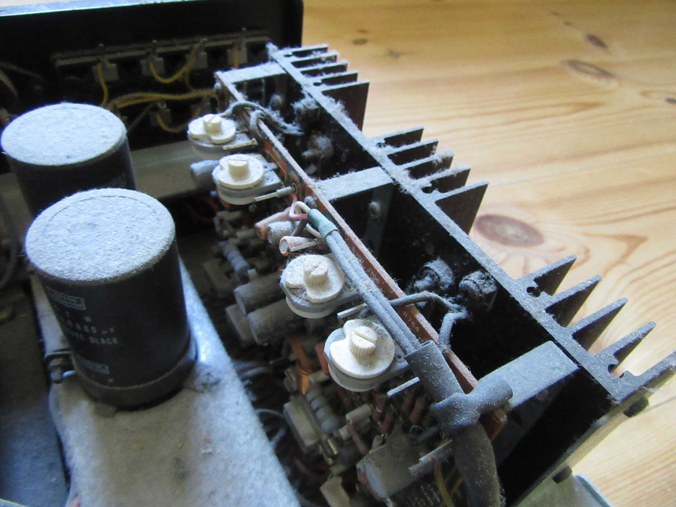
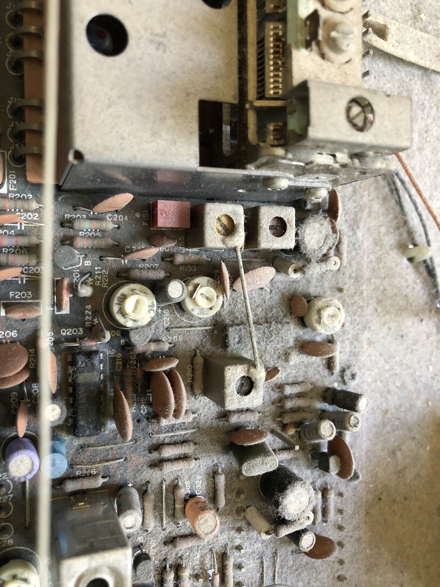
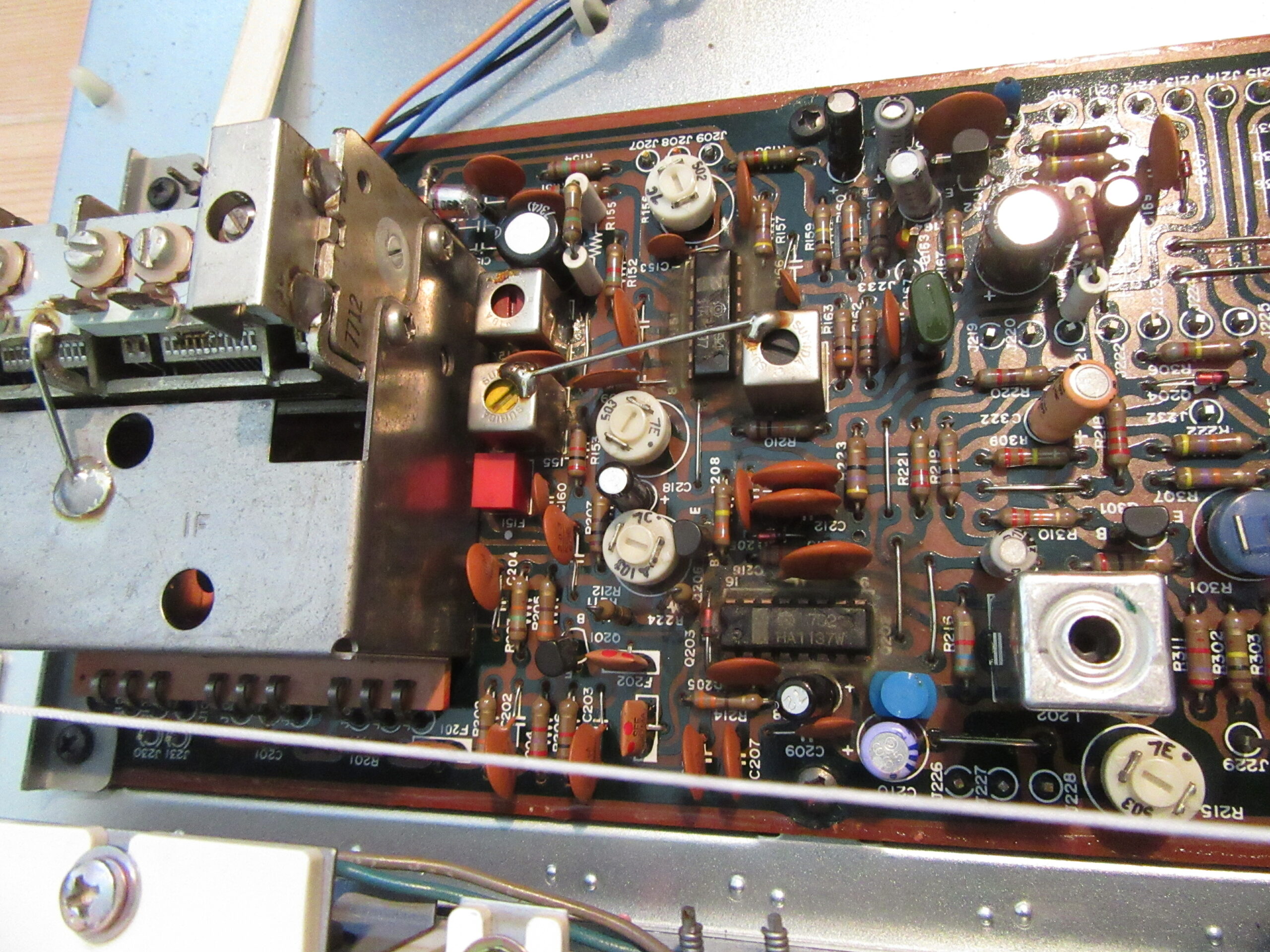
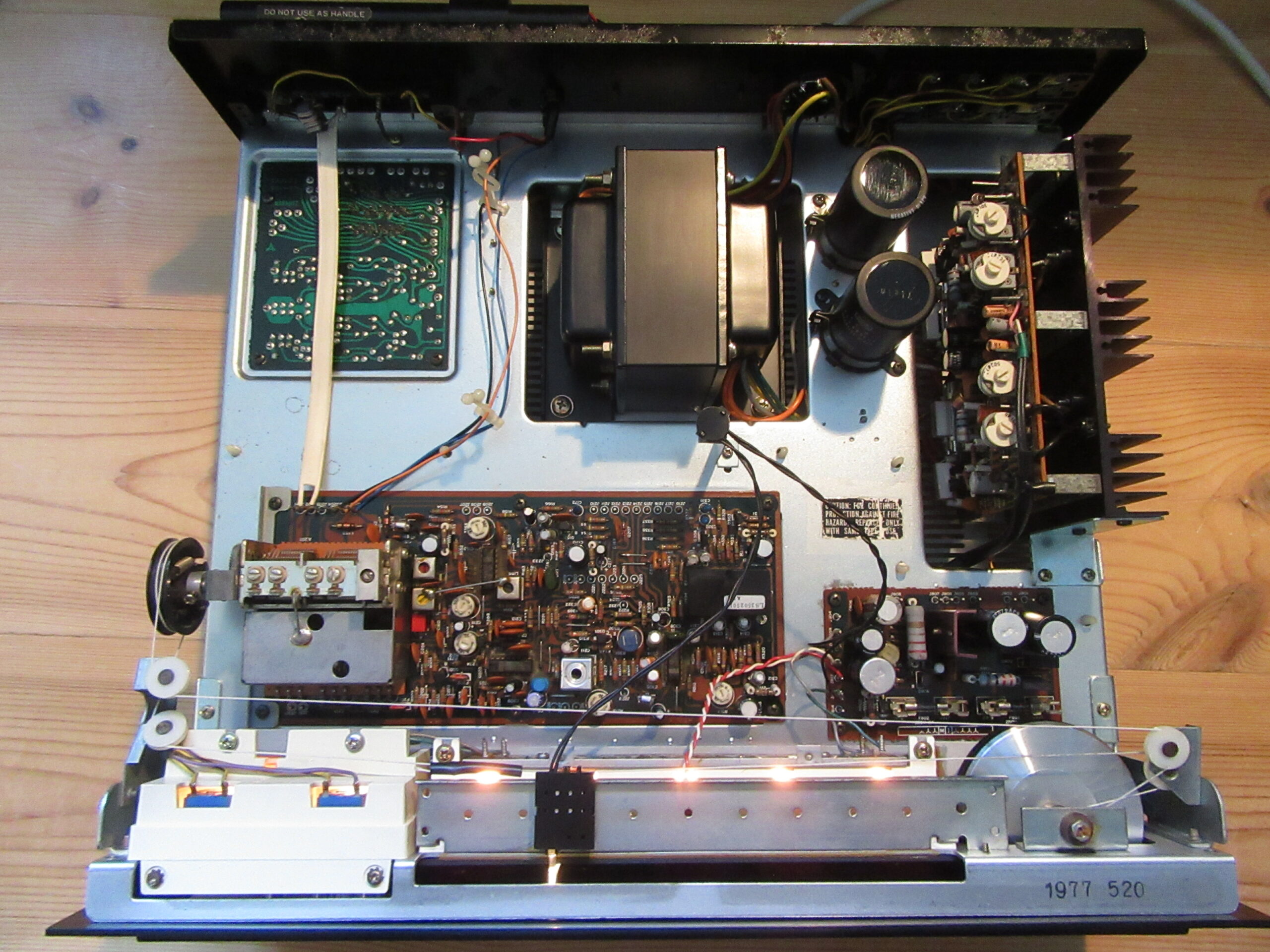
CPU boardCPU board close up Dallas chips
In the case of the oscilloscope here, a failure of the two ICs would mean that calibration data and information about enabled additional functions would be lost. After all, the built-in batteries lasted from 1997 to 2021. With ten years of guaranteed life, that’s almost two and a half times the time.
Data backup
First, it’s a good idea to make a backup of the NVRAM contents. The device has a built-in 1.44MB HD floppy drive. Fortunately, someone wrote some scripts and posted them here that allow you to back up the NVRAM to a floppy.
For me the whole thing worked flawlessly on the first try. I used the tool “tdsNvramFloppyDumper”. Later I used the programmer to write the data to the replacement chips.
Desoldering
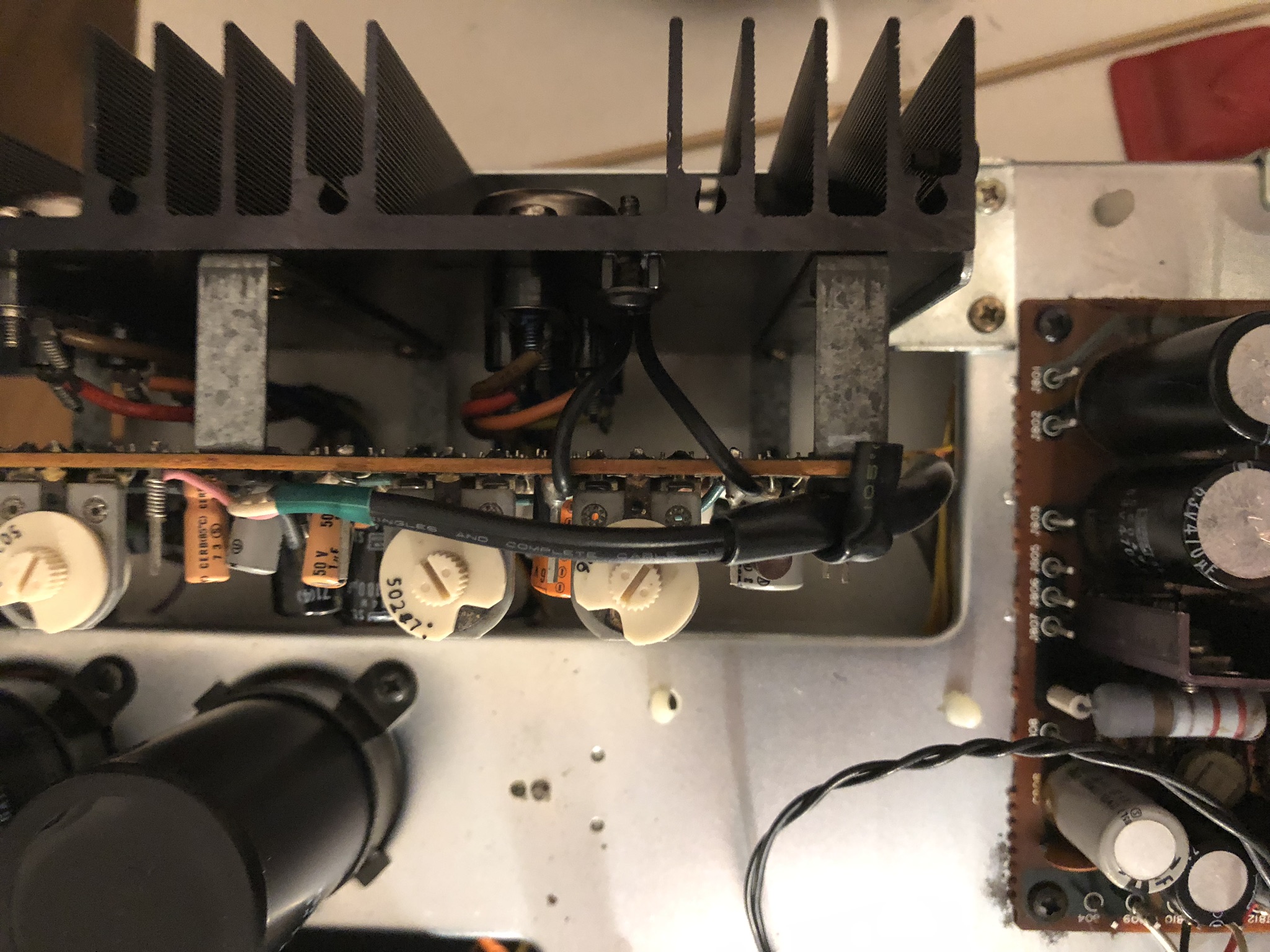
Now it was time to desolder the old parts. The oscilloscope is built very service friendly. To remove the CPU board, no instructions are necessary in my opinion. The desoldering itself I always do with this somewhat larger manual desoldering pump and a normal electronic soldering iron.
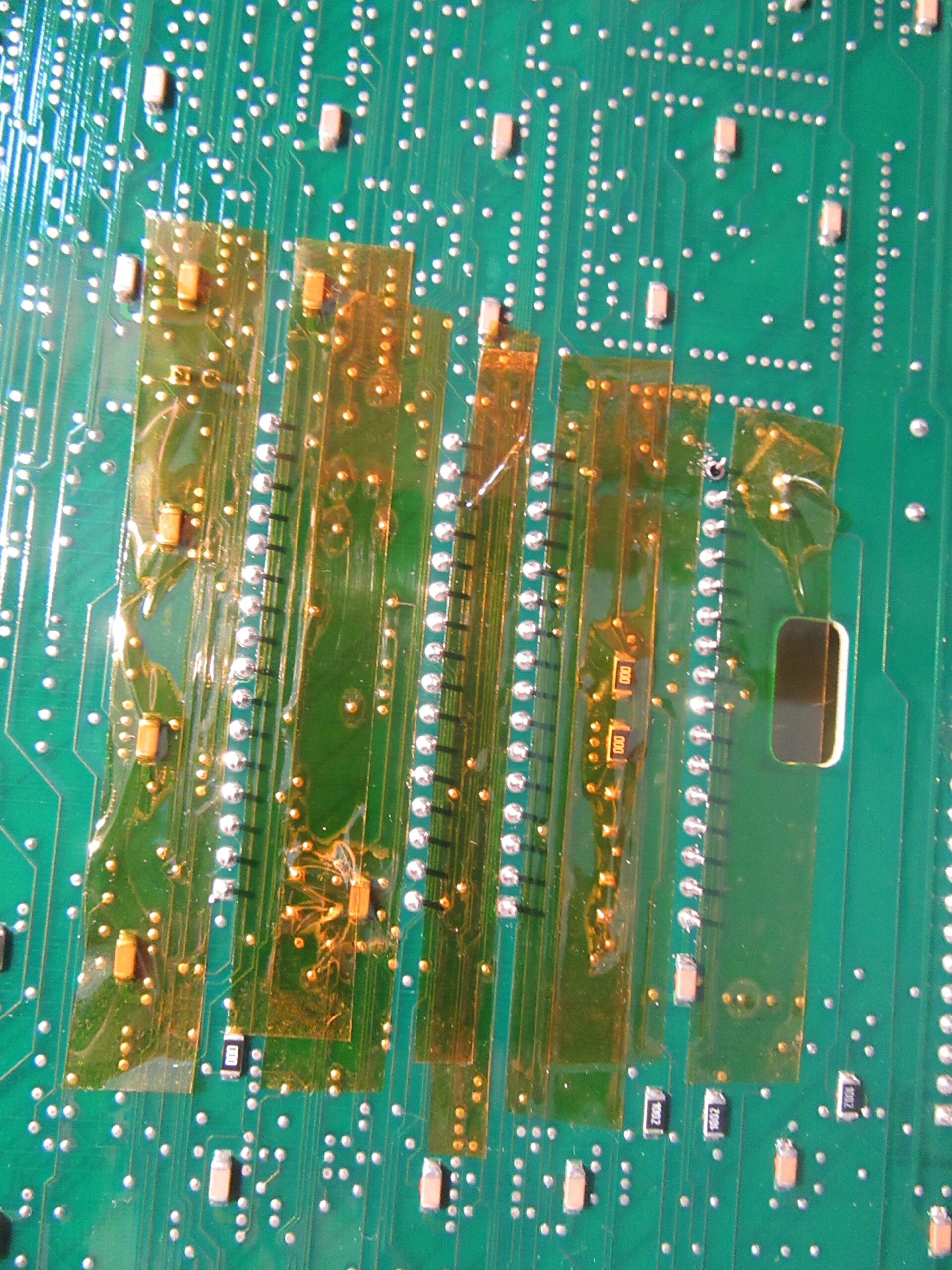
Surrounding area masked with tape
It is important to protect adjacent thin conductors with Kapton tape. The recoil of the pump throws the soldering tip a little bit away when triggering. This occasionally destroys thin conductors next to the solder pads. The tape reliably prevents this in my experience. The desoldering worked fine, I also had only one attempt.
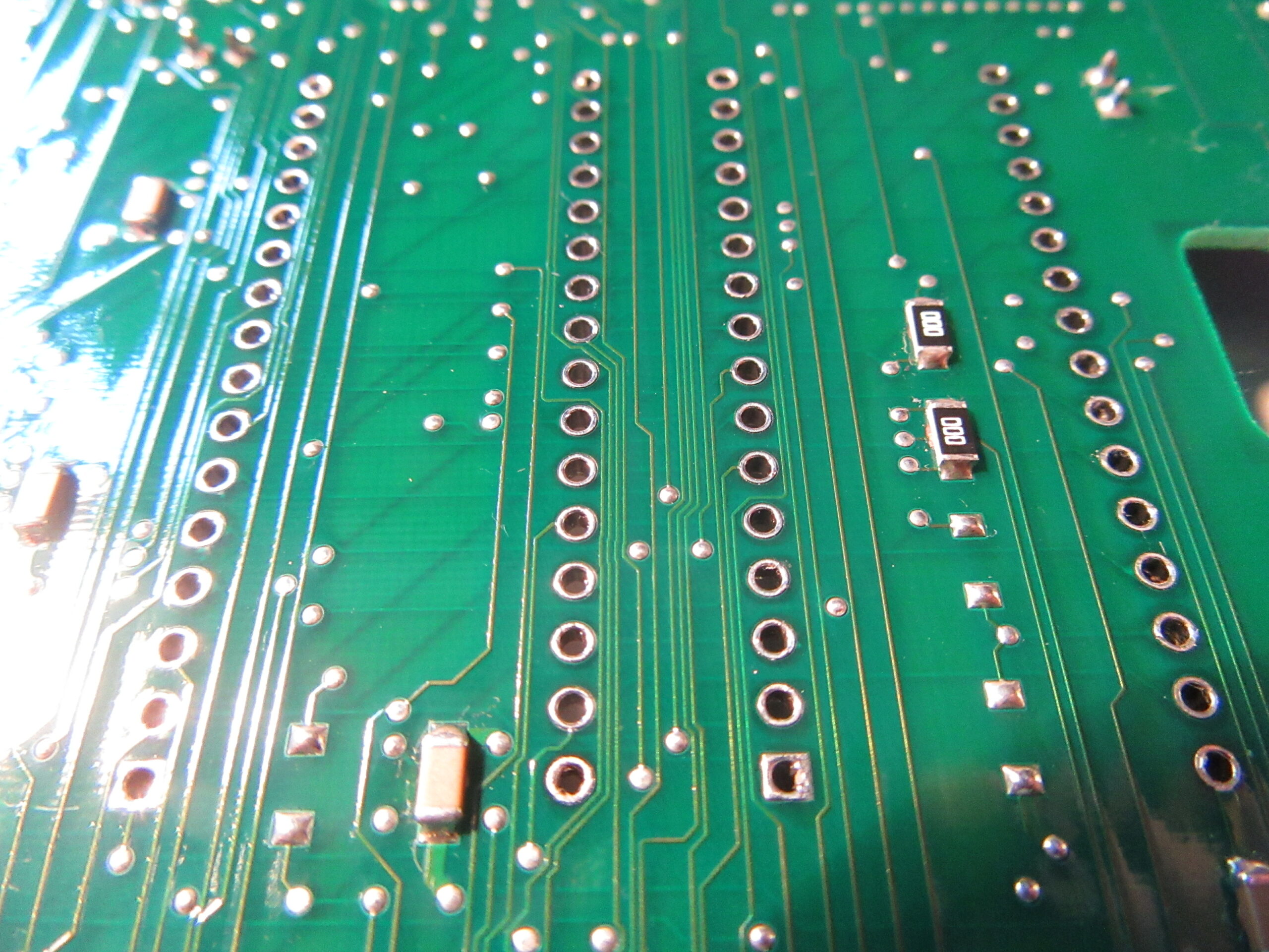
Close up Kapton tape for protectionBoth Dallas ICs desolderedFreed solder pads close up
Exchange parts
DS1486
The RTC is the more difficult part. I was lucky and found a ready-to-use rebuild instructions on the net as well as a remaining stock seller from China, who sells the obsolete DS1384G, which is necessary for the replacement. Nevertheless, be careful with the purchase, also from this IC all kinds of fakes are traded.
Rebuilding the small module was easy. During testing I learned that both batteries must be connected for the RTC to work. At first I had tested this only with the primary battery.
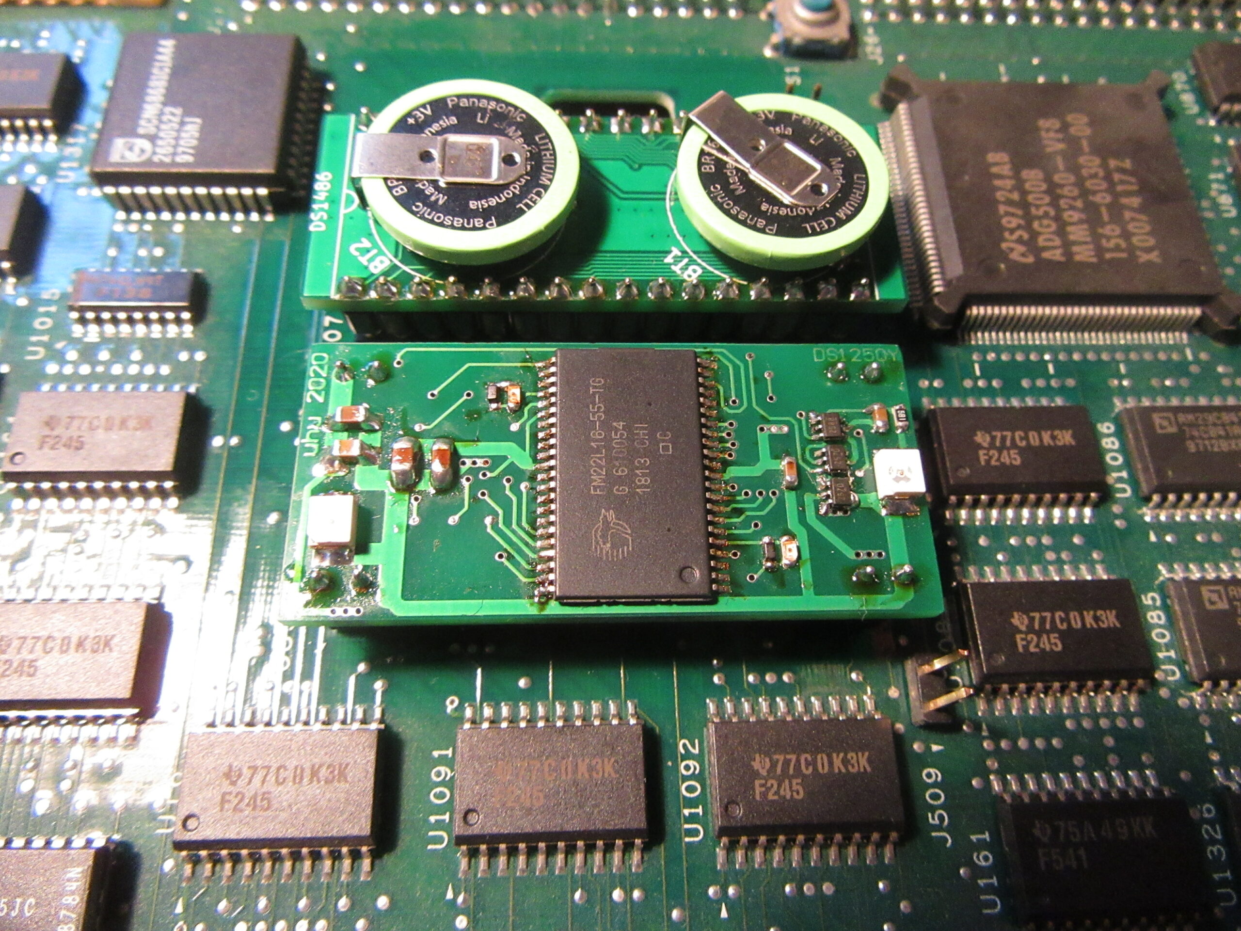
DS1486 Replacement module with batteriesDS1384G hidden under one of the batteriesDS1486 Replacement module from below
Another thing worth mentioning is the choice of batteries. There are six different common lithium battery technologies and some exotic. All have different voltages, advantages and disadvantages. In this case here it is important that the self-discharge is low and the capacity is high. This guarantees a long service life. The type “BR1632A/HAN” from Panasonic used here is a lithium carbon monofluoride battery, which meets these requirements.
DS1650Y
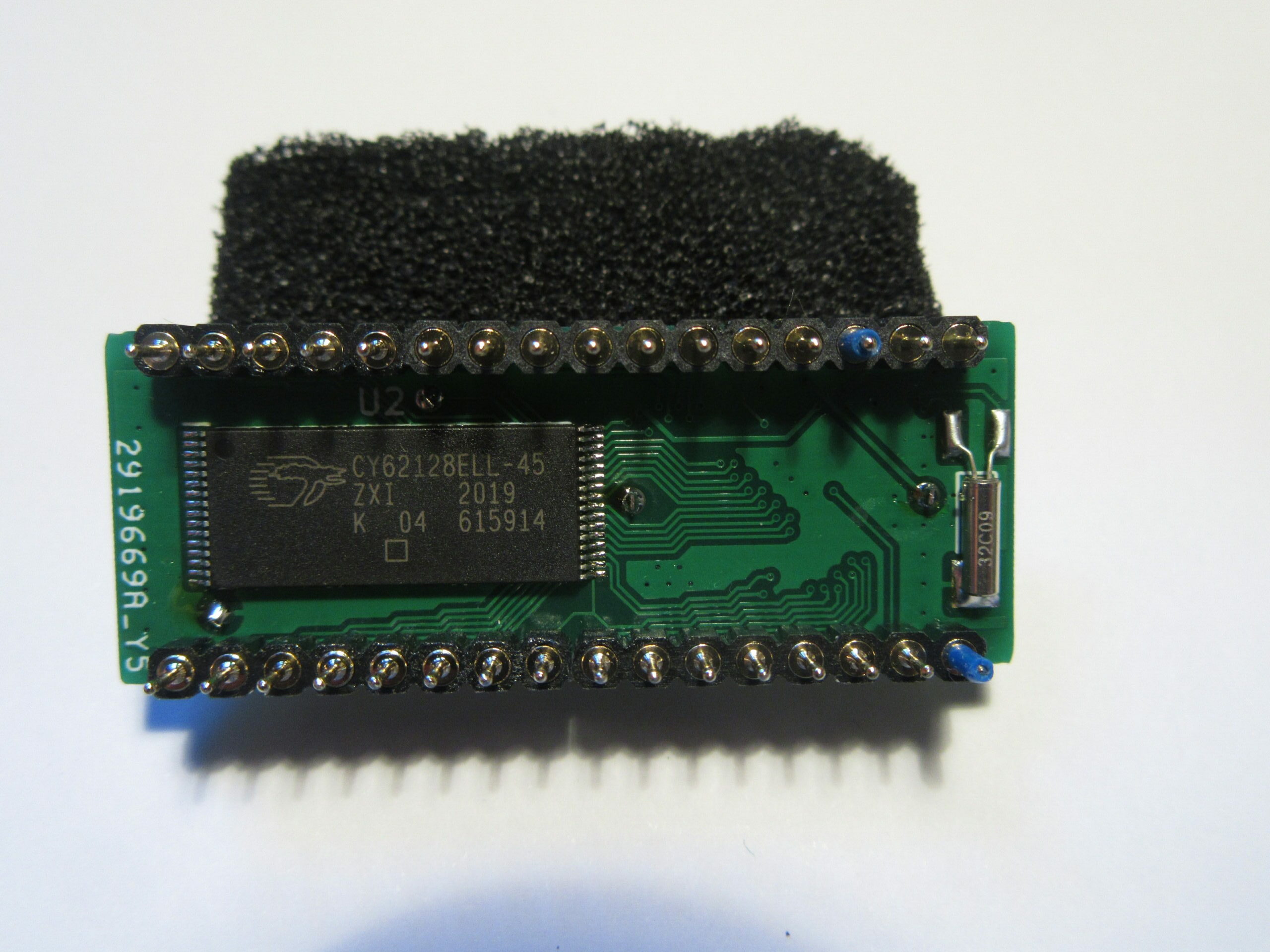
The replacement based on a FRAM for the 4MBit NVRAM DS1650Y I developed myself at the beginning of this year. It is described in detail in the article. In the TDS754C a DS1650Y is installed, but the write protection feature of the component is not used. The replacement with the FRAM module is therefore possible.
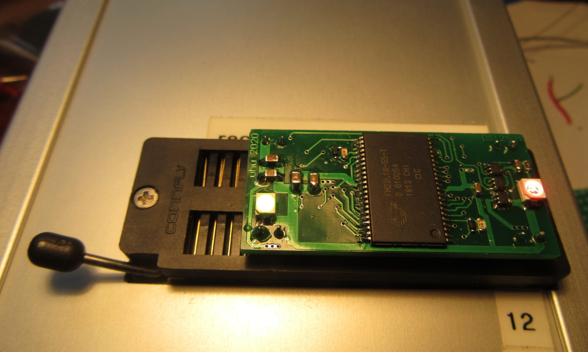
DS1650Y FRAM replacement module
Installation
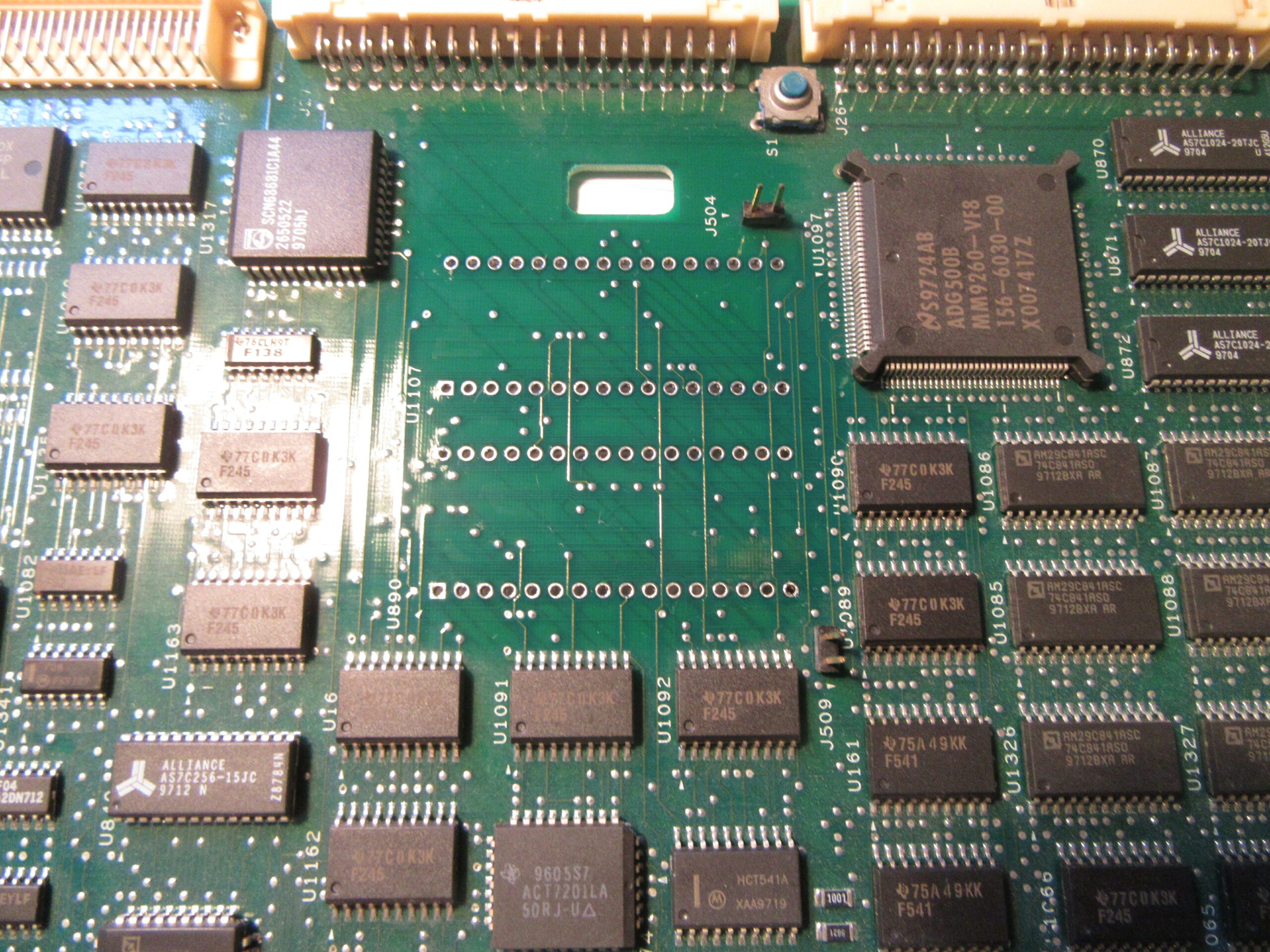
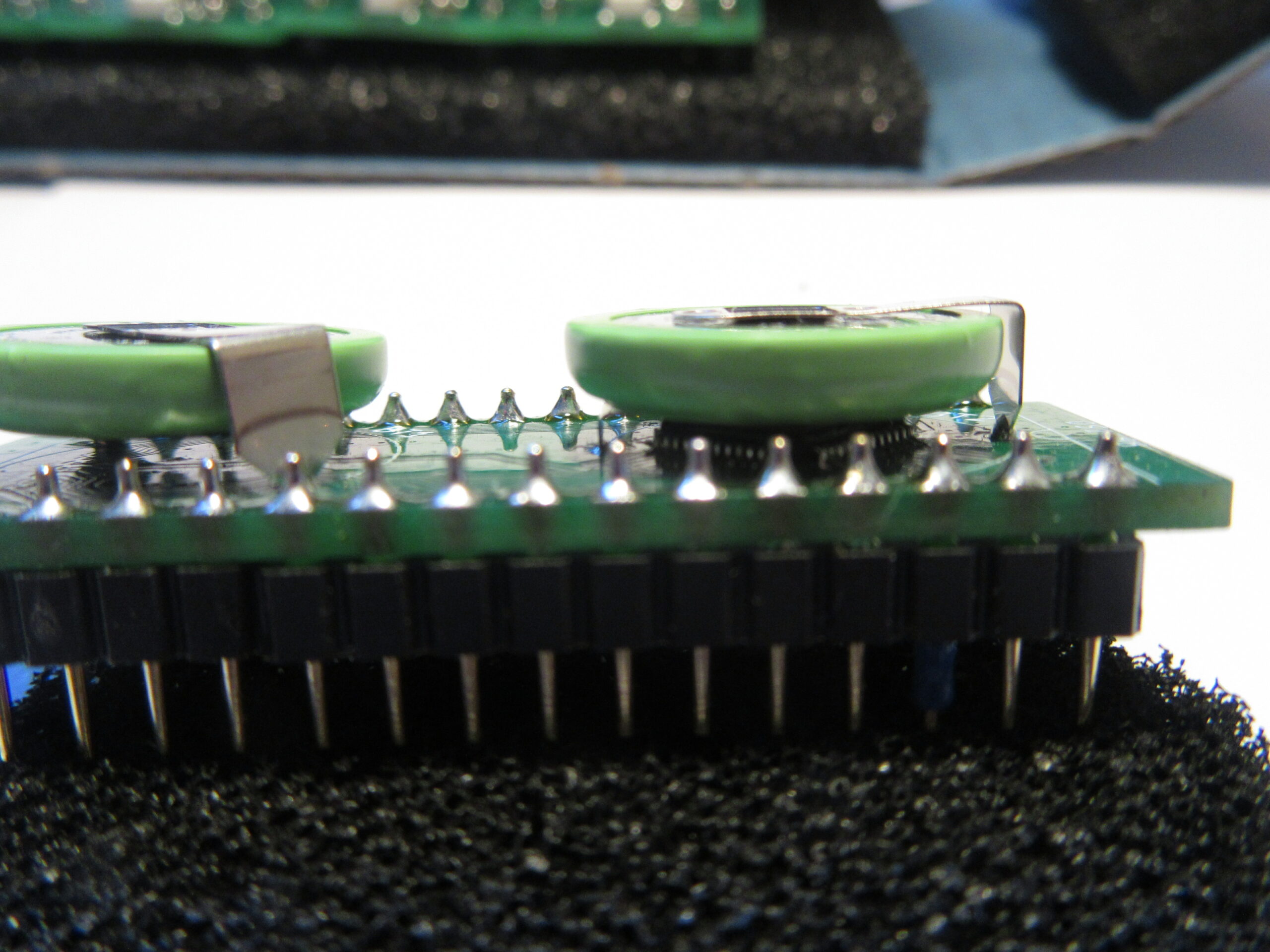
The new components are conveniently socketed. This makes it easy to remove the modules to replace the batteries, for example. Besides, it was uncertain whether the exchange would work. In case of problems, I could have simply put the two soldered out parts back into the socket.
As sockets I use some with a low profile. The contacts are partially recessed in the board. This makes the replacement part with socket only slightly higher than the original.
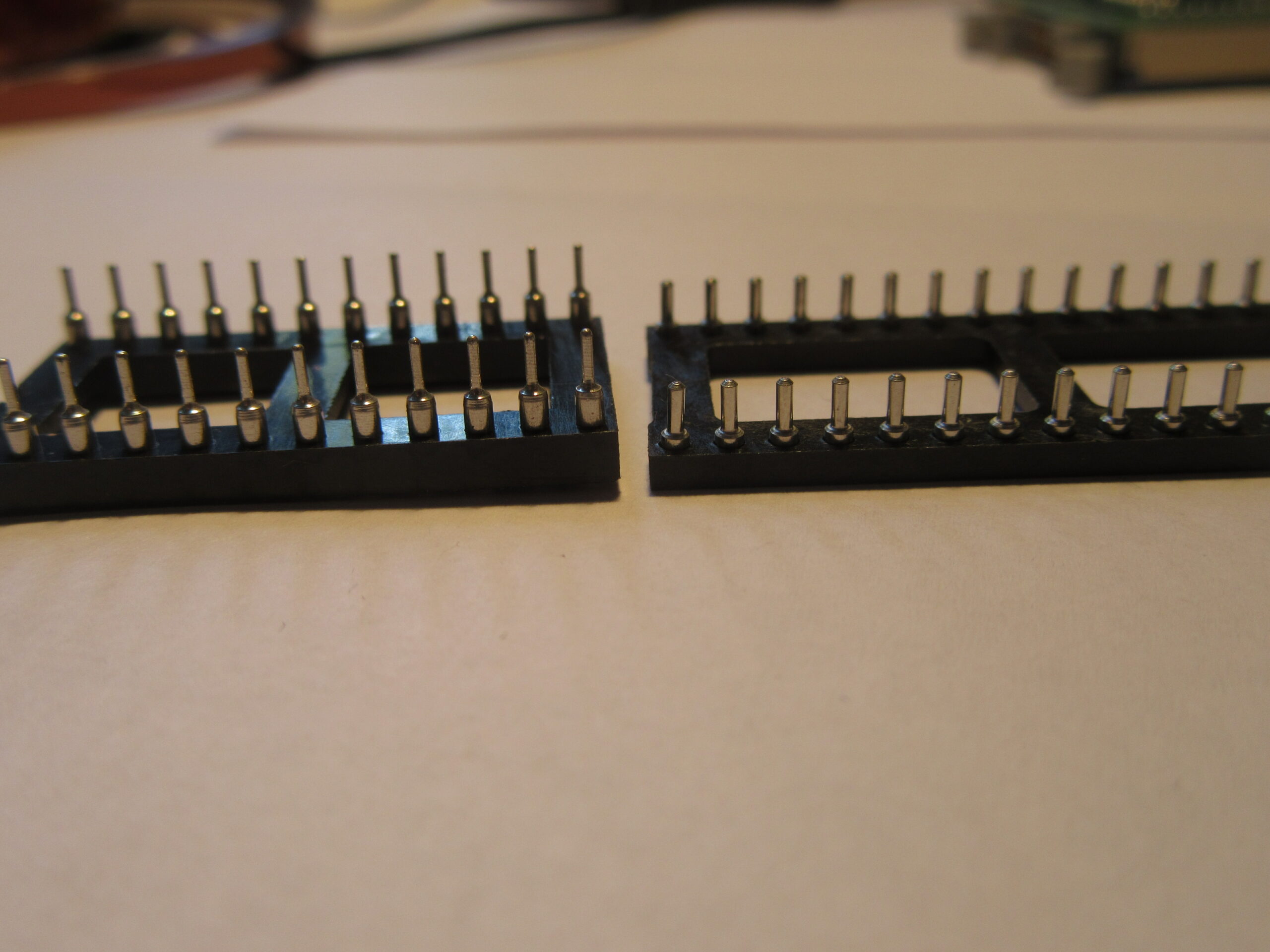
Left standard socket, right low-profile version
The two sockets were quickly soldered in place. It was annoying that the pin headers of the two replacement modules were a bit too thick. Thus they do not fit completely into the socket and are relatively difficult to insert and remove. I should have read the data sheets of the mechanical components beforehand.
Socket ready solderedSpare modules equipped
Putting into operation
First, the device reported an NVRAM CRC error after power-on. Maybe the memory was written during the backup which leads to an invalid checksum. The attempt to restore the backup with the above linked “tdsNvramFloppyTools” was successful. The device now starts again as usual and at least the two replaced parts will do their job for many more years.
This project is not very big but still something special. On the one hand it is part of a restoration which has been prepared for years. On the other hand it seems that nobody has come up with the idea to replace a 5V NVRAM with a 3.3V FRAM or to publish it.
Problem components NVRAM
If you want to keep old devices for a long time, you will always come across chips with integrated lithium battery from “Dallas Semiconductor”, which was bought by “Maxim Integrated” in 2001, which in turn was bought by “Analog Devices” in 2021. These are mostly NVRAMs (non-volatile RAM) or RTCs (real-time clocks) with NVRAM. The battery integrated in the chip package enables the data in the RAM to be retained even after the operating voltage is switched off and the RTC continues to run. An NVRAM controller, which is also integrated, takes care of switching between battery and operating voltage as well as data protection when switching on and off.
Basically, this is a very practical solution, since one can use a single component instead of a whole circuit including battery. However, it is fatal when the built-in battery is exhausted after about 20 years. Almost always the whole device is no longer functional. The components are of course no longer produced. Also the remaining stock traded on the Internet is either already too old or even more often faked. I have bought two fakes myself. Thus, replacement with the original part is not an option.
Soldered NVRAM and RTC (Tektronix TDS754C CPU Board)
Replacement options
The replacement of RTC and NVRAM differs significantly.
The NVRAM can be replaced by a corresponding SRAM with NVRAM controller and battery. Some examples can be found on the net.
Another variant is the replacement by FRAM, a memory which can be written arbitrarily like RAM, but which keeps the content even without operating voltage. There are also examples with the FRAM types FM16(W)08 and FM18(W)08 with 64kBit and 256kBit size respectively. The charm of this solution is that no battery is necessary and thus the memory remains maintenance-free. Unfortunately, the two mentioned FRAM types are pin-compatible with the Dallas NVRAMs, but they are controlled somewhat differently. Thus the exchange unfortunately does not work in all devices.
An RTC cannot be replaced so easily. The RTC maps the time to a memory area that is accessed like “normal” RAM. The chip has to keep the required timing exactly. This can only be ensured by using dual-port RAM. However, I have not found suitable circuits. This would be a small project for the future. Currently, there is only the possibility to mechanically drill out an old RTC and connect a new lithium battery from the outside. Or you can use a compatible RTC chip, which is still available as residual stock. As far as I know this is only possible for a DS1486, which is replaced by a DS1386G incl. RAM and battery.
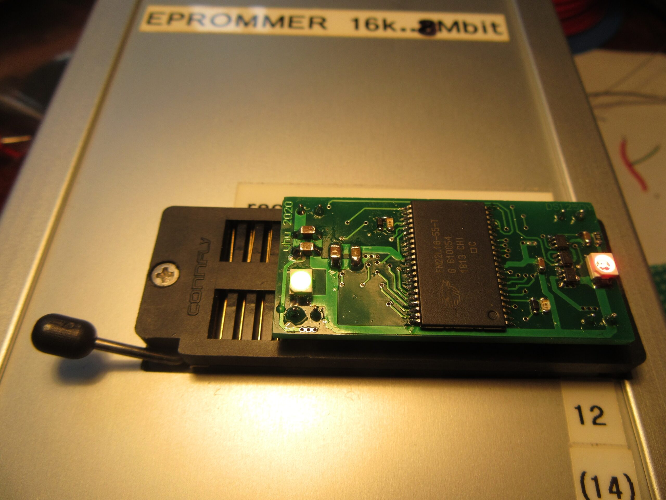
DS1250Y/DS1650Y FRAM Replacement
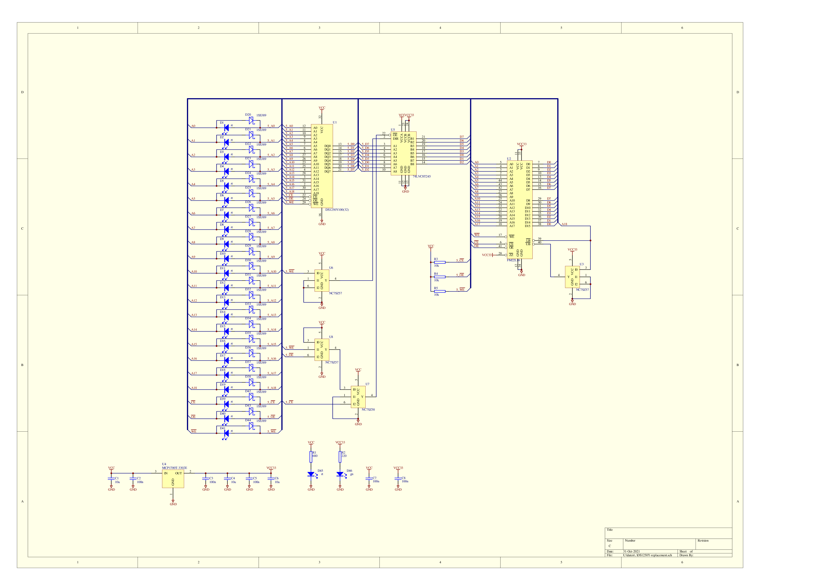
Now to the corpus delicti. The DS1250Y component from “Dallas Semiconductor” is a 4MBit NVRAM. The pin-compatible DS1650Y variant also has the option of write-protecting individual memory areas via software. Thus the DS1650Y can replace the DS1250Y. The other way around, this doesn’t work in every case, but only when the software doesn’t use the write protection feature or doesn’t depend on it.
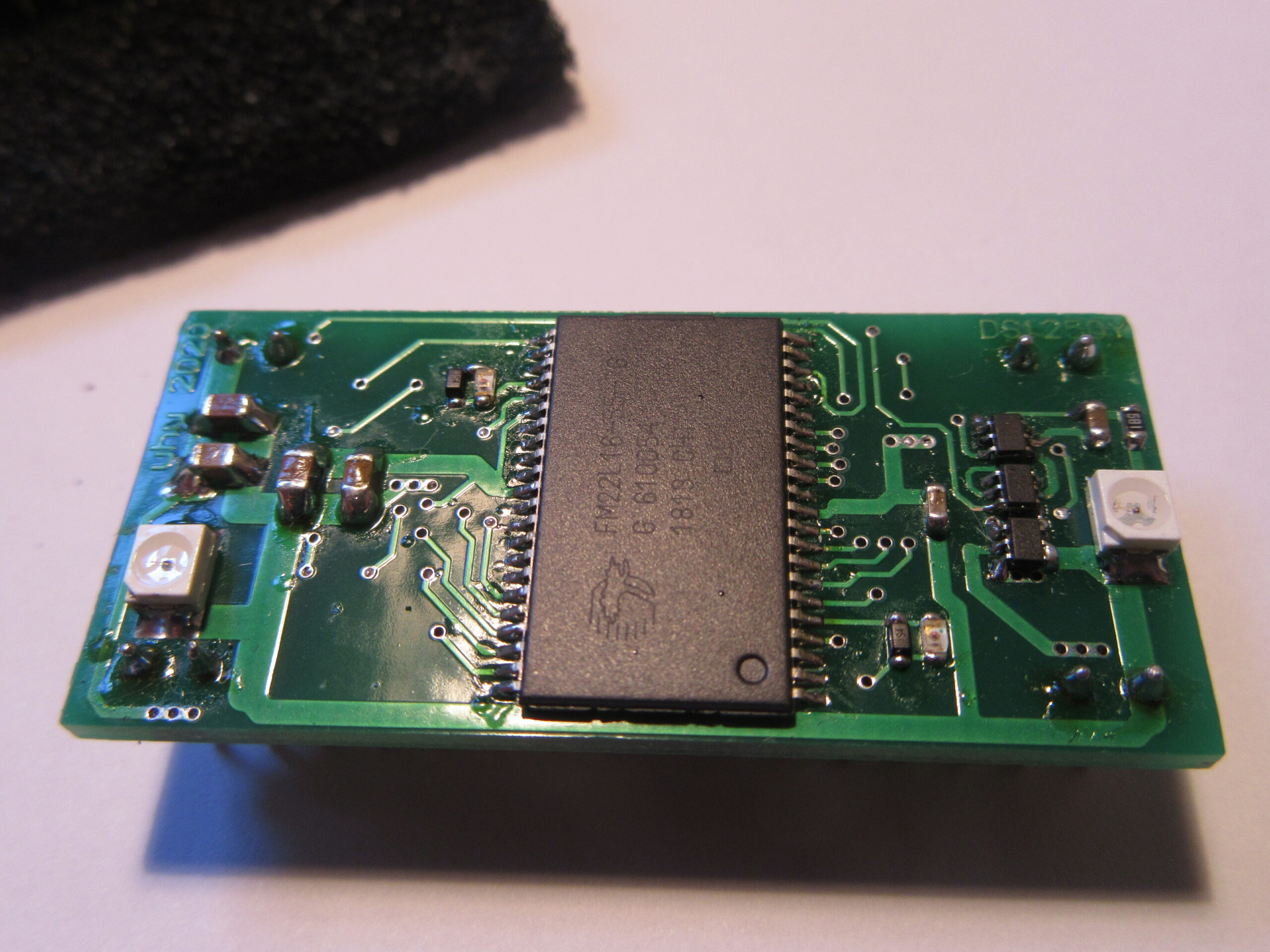
A short component search for parallel 4MBit FRAM brings only one product to light, the FM22L16-55-TG. Unfortunately, it works with a maximum of 3.3V and has 16 bit data width in contrast to 5V and 8 bit on the DS1250Y.
So there are still some parts missing to adapt the FM22L16: Some logic, level shifter, a voltage regulator and some brain power. Difficult in the design was also that the whole circuit has to fit on a board with the size of the original part.
Circuit
After a couple of days of reading and understanding data sheets and drawing schematics, the circuit was ready.
Circuit diagram
I used a bidirectional level shifter 74LVC8T245 for the data bus, a MCP1700T-3302E low dropout voltage regulator for the 3.3V power supply, a couple of universal single gates for the control logic and Schottky diodes and LEDs for the unidirectional level shifters of the address and control lines.
In the first version I had forgotten the pull-up resistors R3 to R5 which caused the data to be changed when the device was removed from the programmer. Otherwise, the circuit works flawlessly and easily meets the timing requirements of the original.
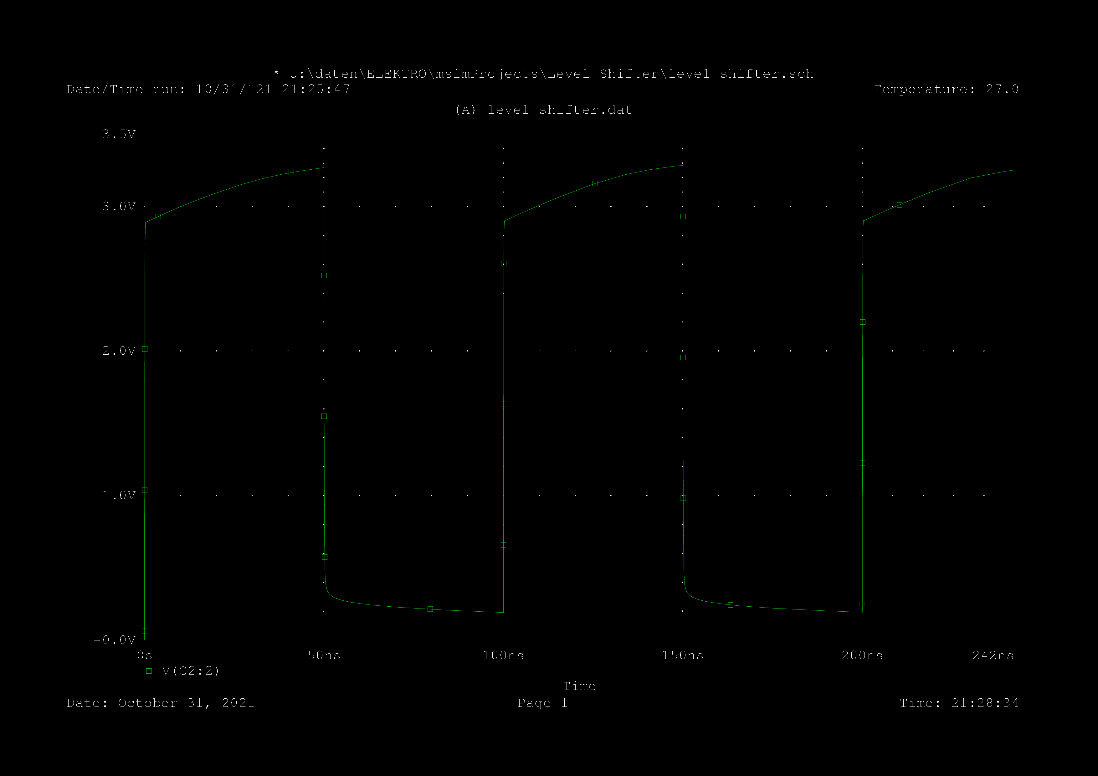
The unidirectional level shifters with a Schottky diode plus LED are still special and grown on my crap. I simulated the circuit and found that this simple way works safely and quickly.
Simulation level shifter for address and control lines
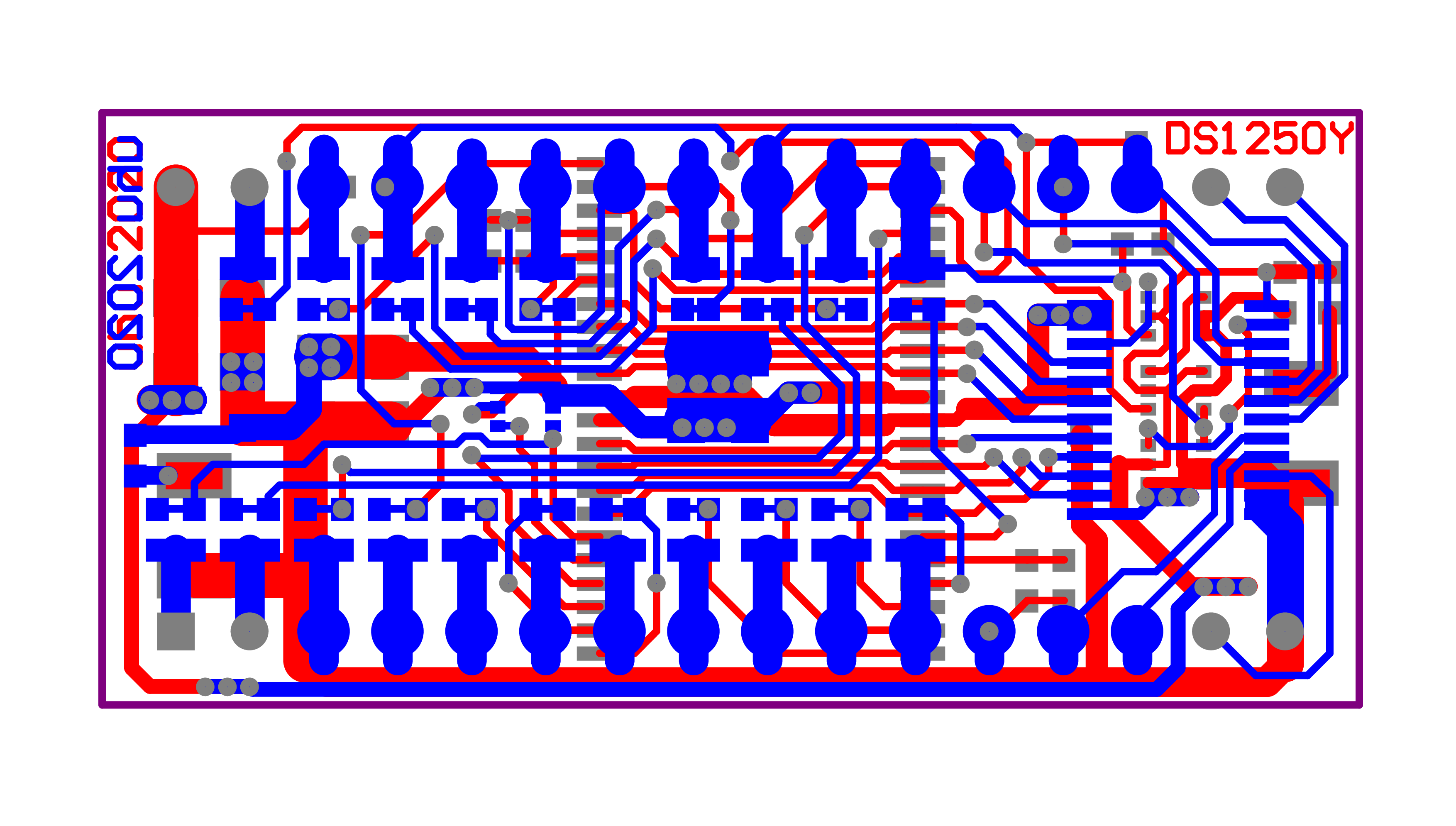
The circuit is placed on a double-sided PCB, which is about 1mm wider than the original component. In most devices, however, there is enough space for it.
Board layout
Gerber Files for private reorder are located here. Usually I order at JLCPCB. There you can simply upload the zip for ordering. The bill of materials and the assembly plan are here.
The rest follows as a short picture story:
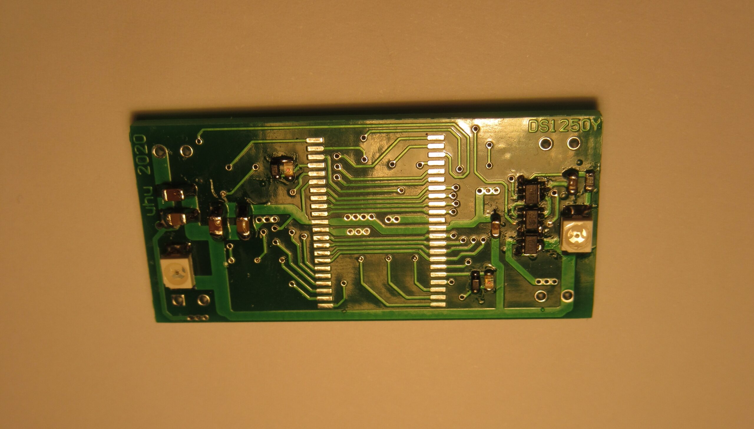
Finished boards are there and are assembledComponents manually assembled and solderedBottom viewBottom view, afterwards added pull ups connected with wire, modification added to published designBottom view, pin header fiddly soldered from besideFirst prototype in the programmer
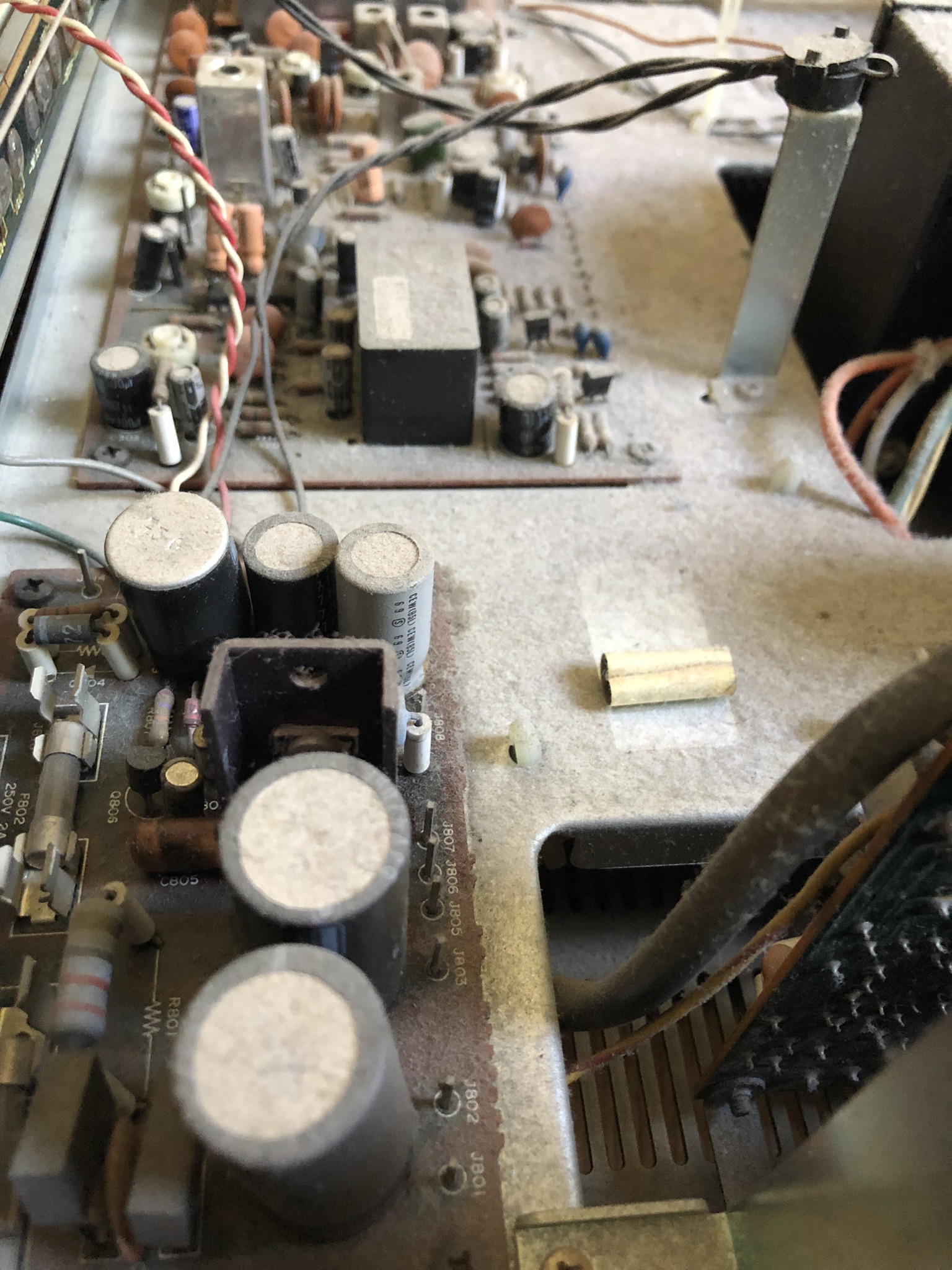
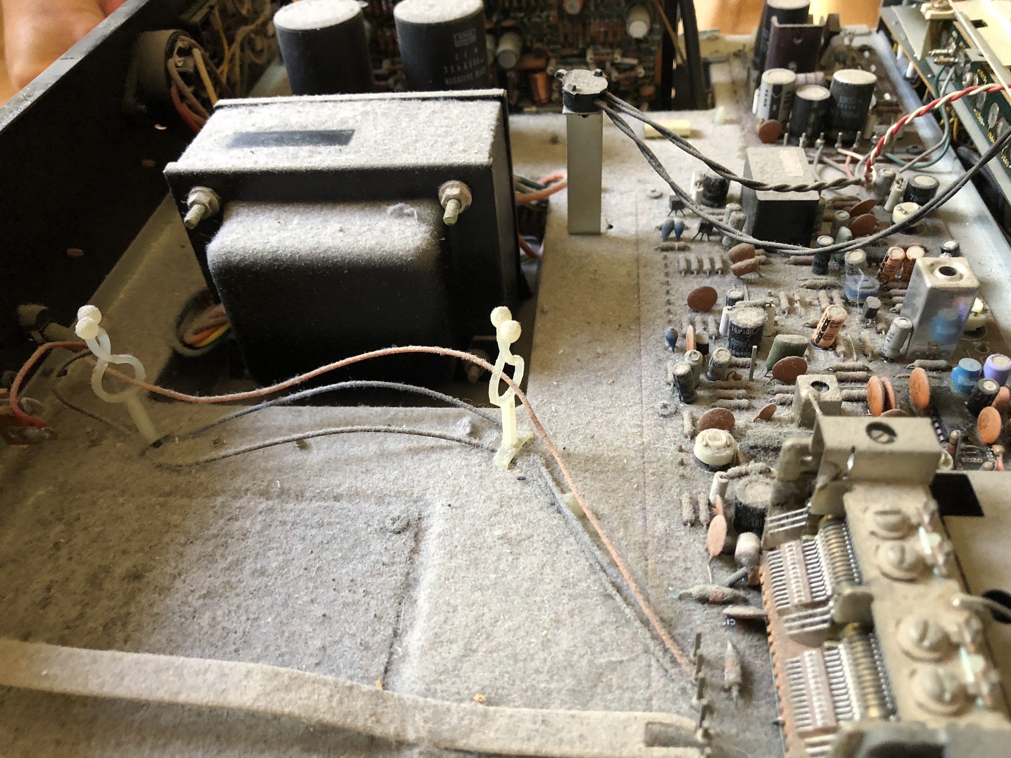
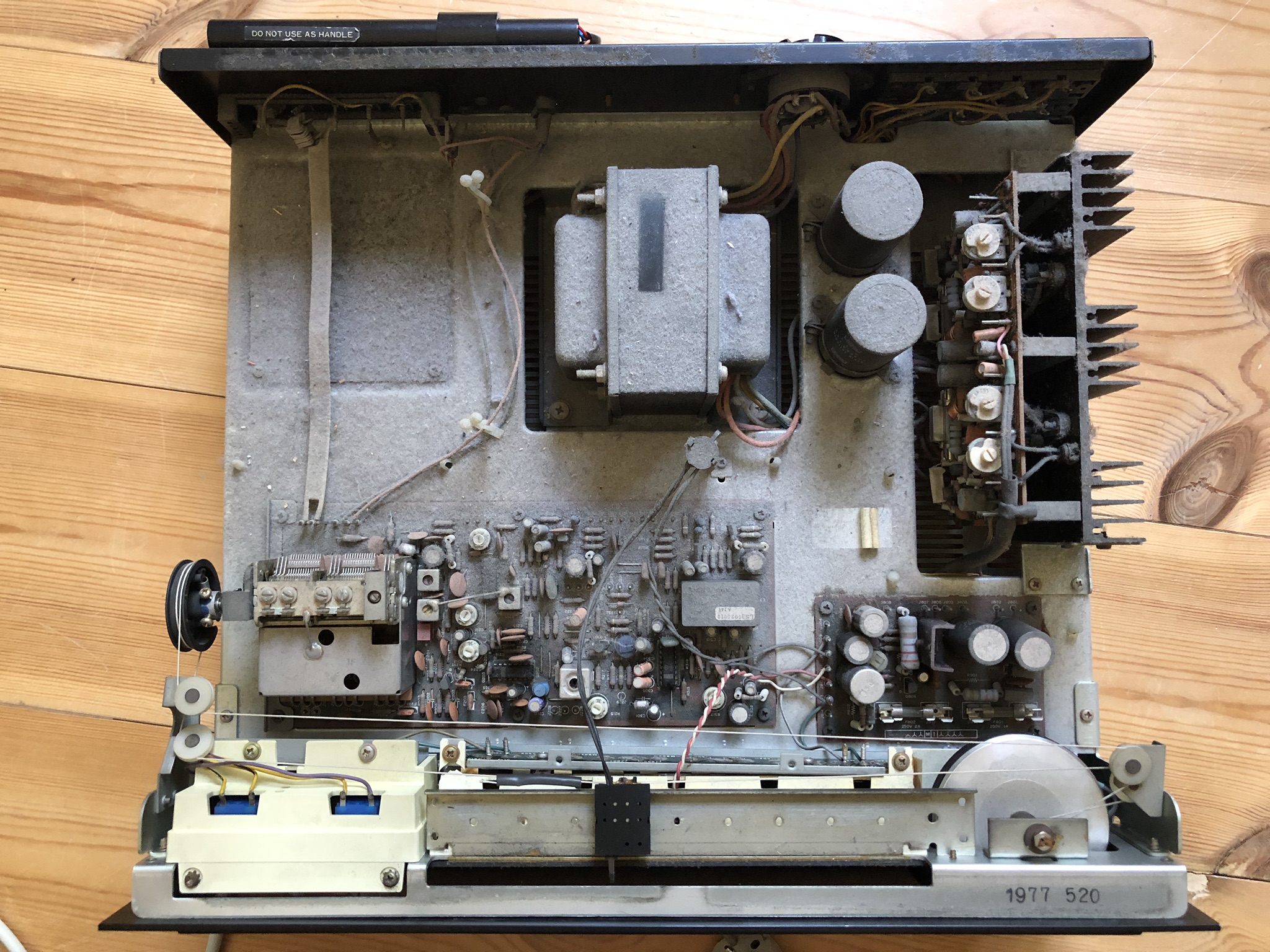
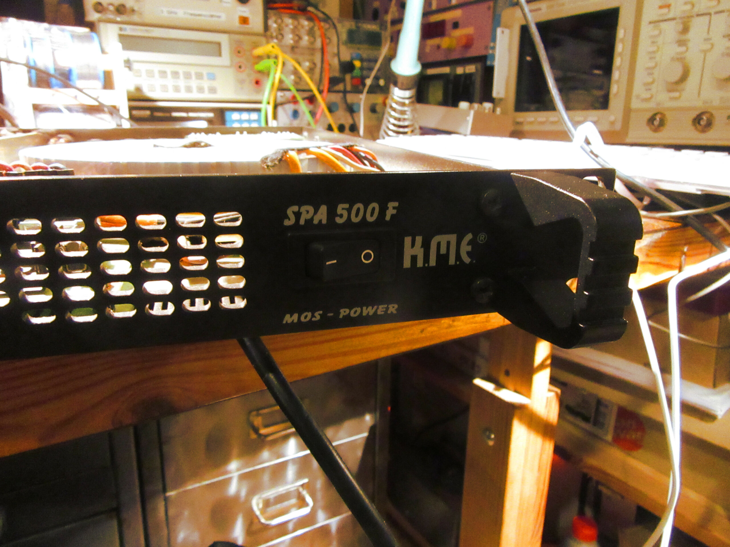
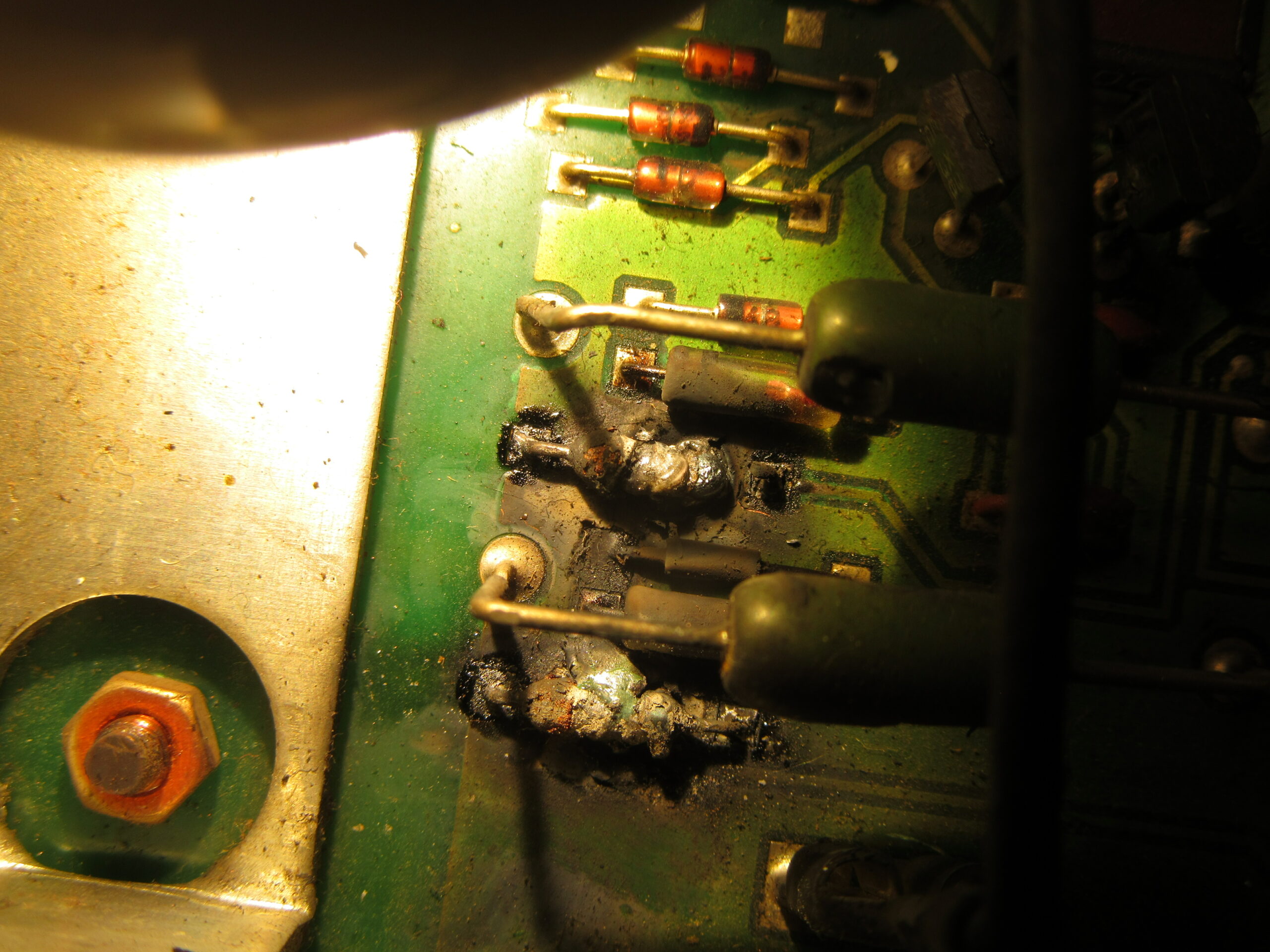
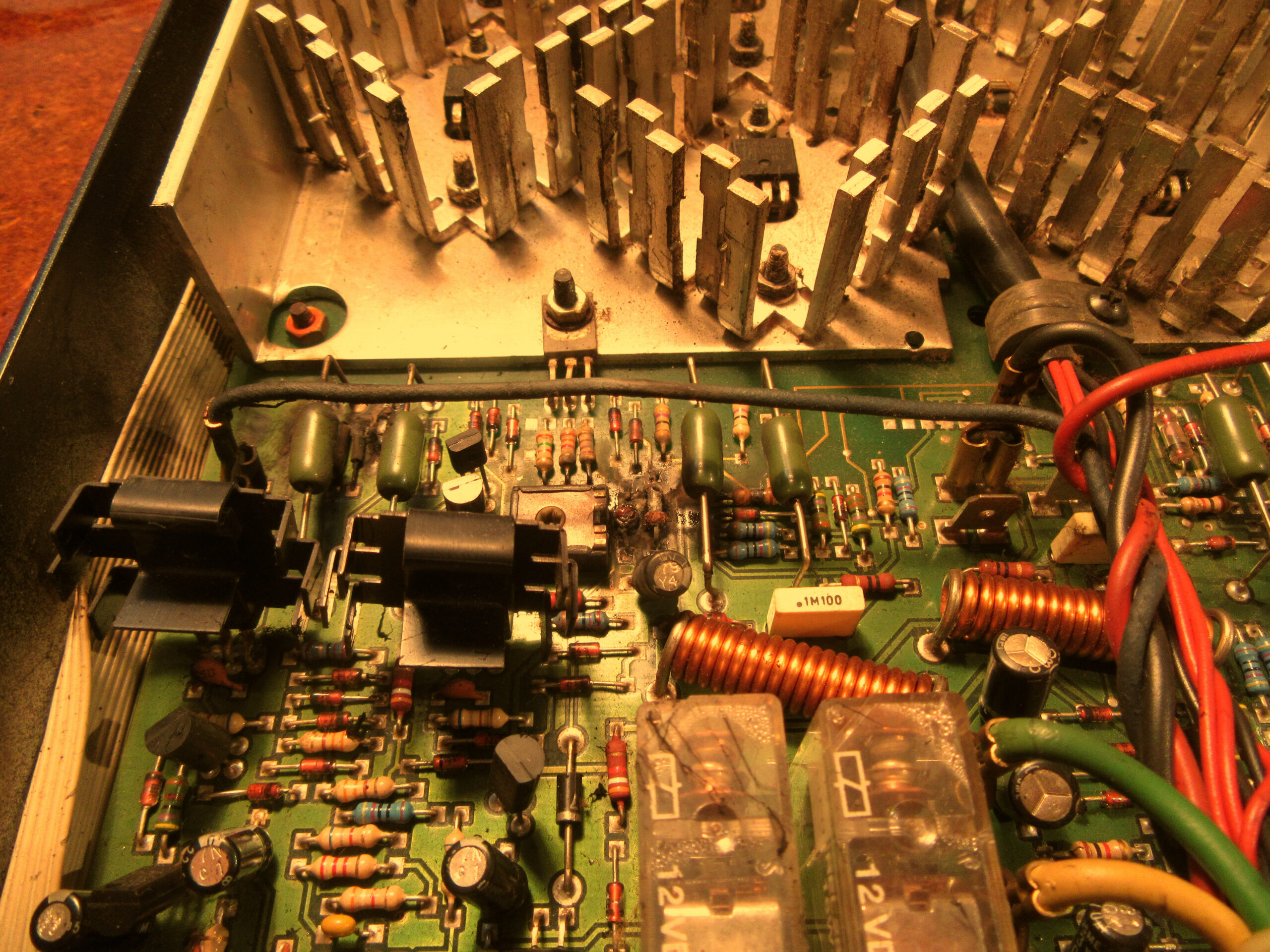
My friend Falk asked me at the beginning of the year if I would take a look at a defective power amplifier that he could buy very cheaply on the Internet. In my opinion, you could not go wrong with it, since the built-in power transformer alone was worth the purchase price. So the power amplifier was ordered and immediately delivered to my home. It was a device from the company K.M.E., model SPA500F with 2x 250W RMS into 4 ohms or 2x 150W RMS into 8 ohms. The year of manufacture was about 2000.The seller described the condition something like this: “One channel does not work, the rest is in top condition, also do not know.” After two days of shipping, the part was with me. The rest of the story I tell as a small picture story below.
Inventory
The first thing to do was the initial inspection, i.e. unscrew the casing cover and take a look.
Housing opened on the workbench
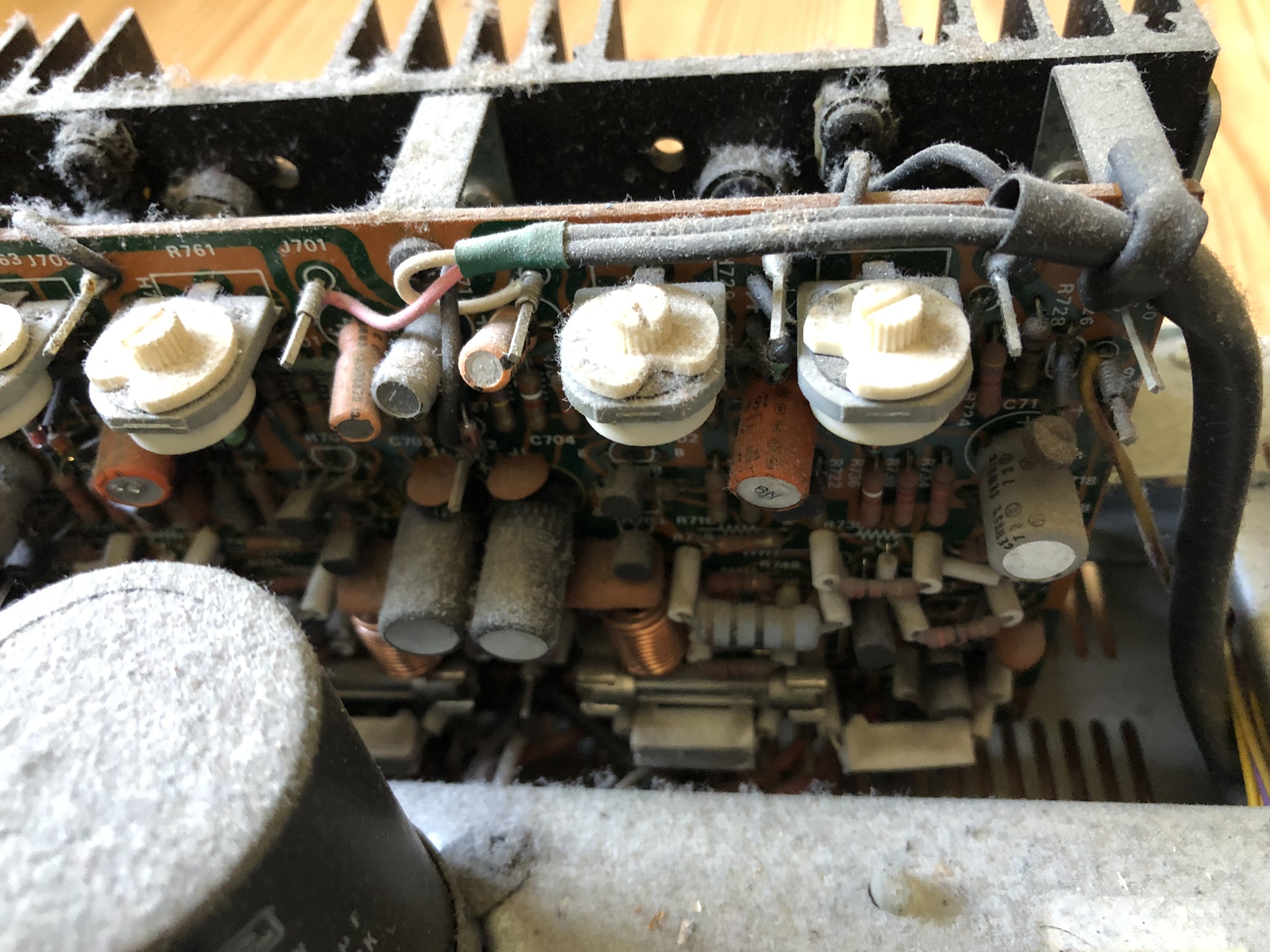
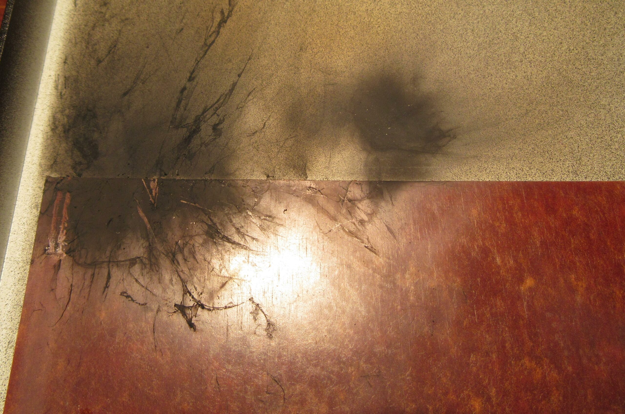
A strong smell of cold cigarette smoke and burnt electronics and corresponding deposits gave away: The device had been used for years in an environment with a lot of nicotine, probably a discotheque.
Brown deposits on the heat sink
In addition, a lot of components on the board had burned or even exploded.
Burn marks in the housing cover
It was also clear that the unit had recently been opened. With the burn marks on the lid and the smell, both of which are hard to miss, the seller may not have been completely honest in his condition description.
Here are some pictures of the exciting parts.
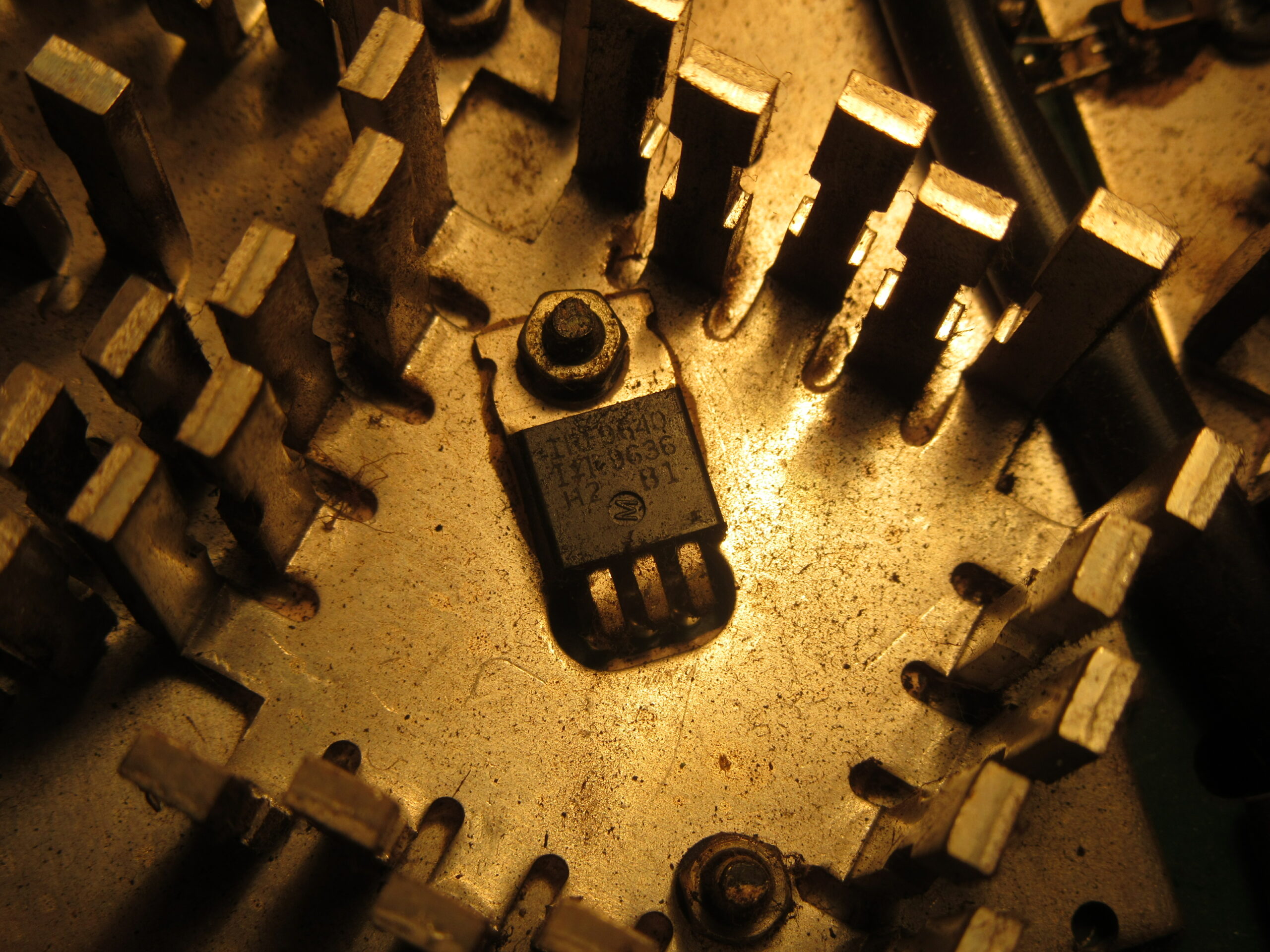
Gate resistors of the output transistorsGate resistors from positive branchMore burned out partsA picture of devastation
Also some traces had dissolved into nothing. It quickly became clear that I would not get anywhere here without a circuit diagram. A search for the documents on the Internet yielded nothing, so without further ado I sent a friendly request to the service email of K.M.E. over the weekend. And voila, on Monday morning, the schematic and assembly diagram were in my inbox, sent by the production manager himself. Many thanks again at this point.
Defective parts
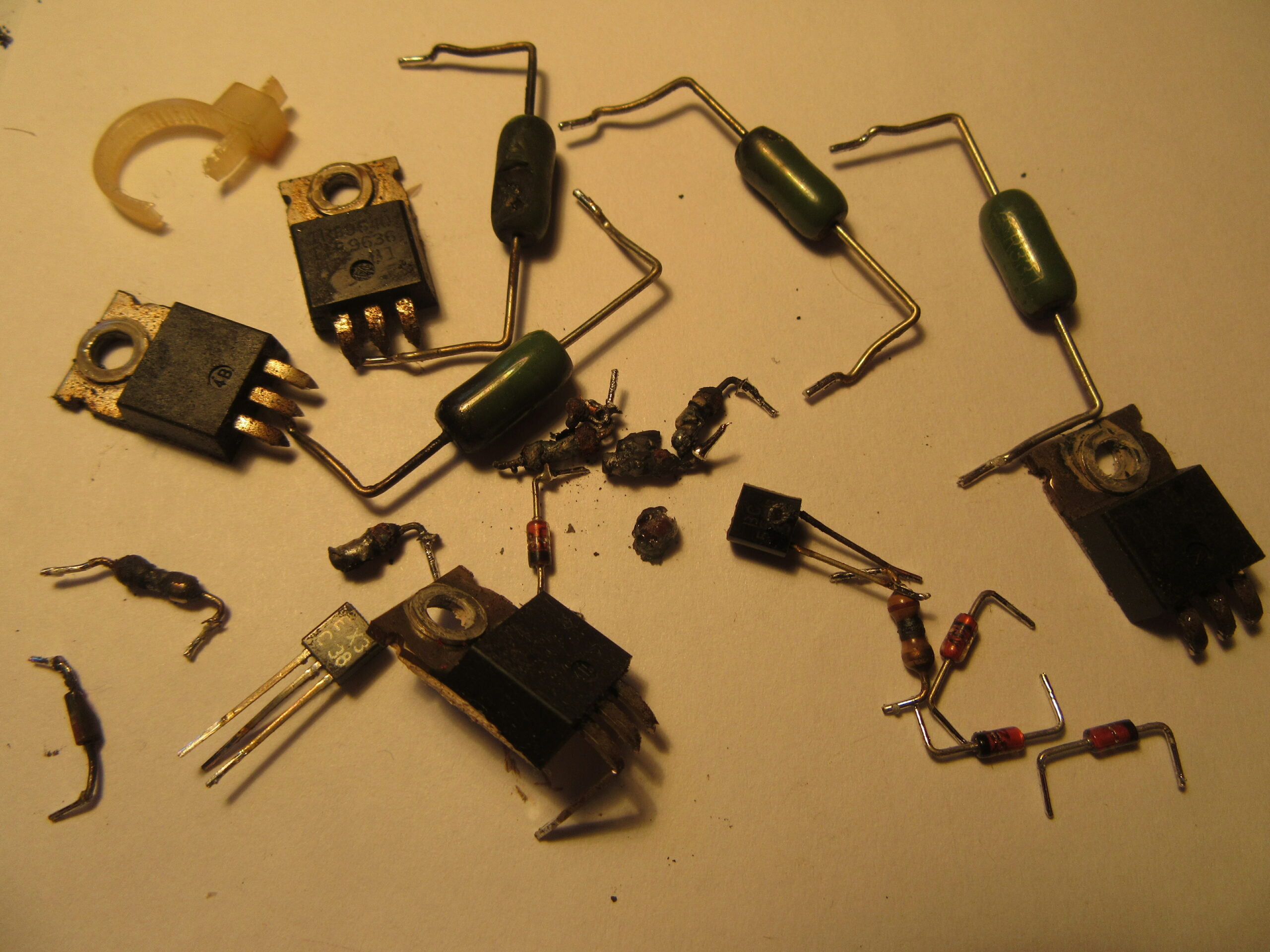
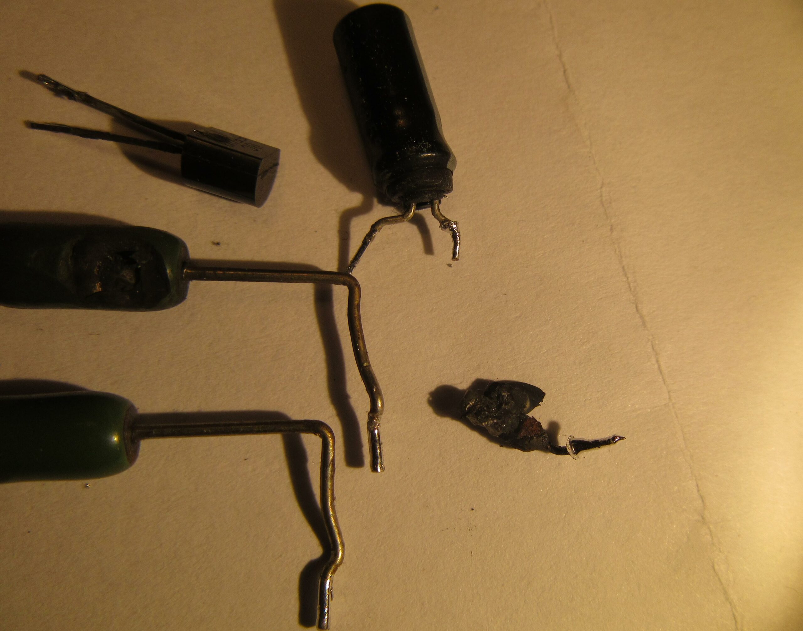
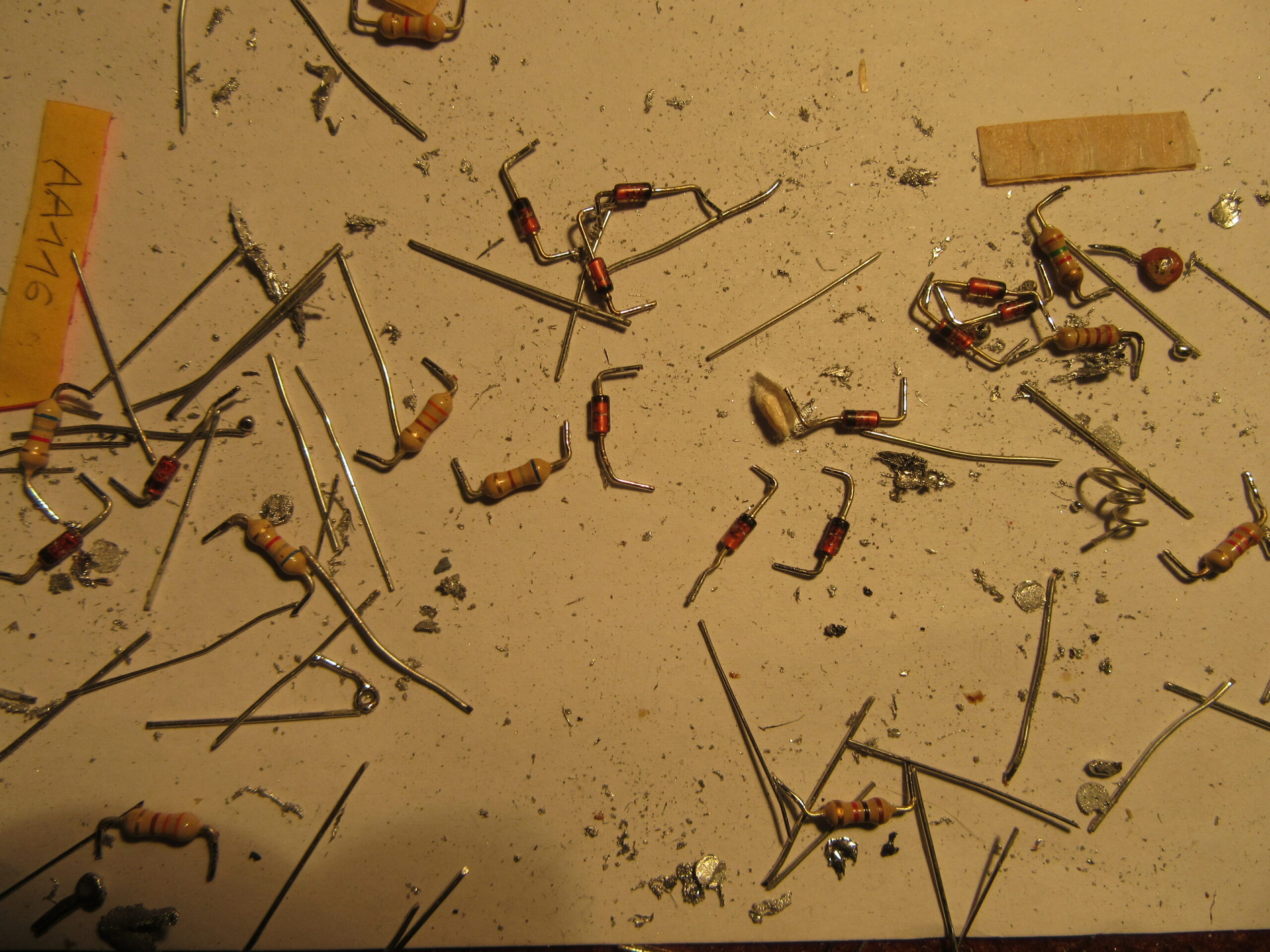
The next step was to find all defective parts and desolder them. As you can see on the photos, a lot of things came together.
Desoldered componentsOther parts
Spare parts
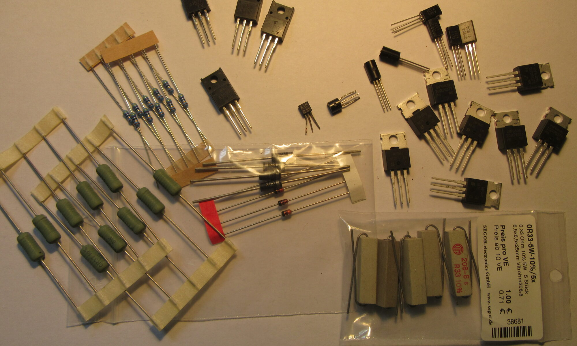
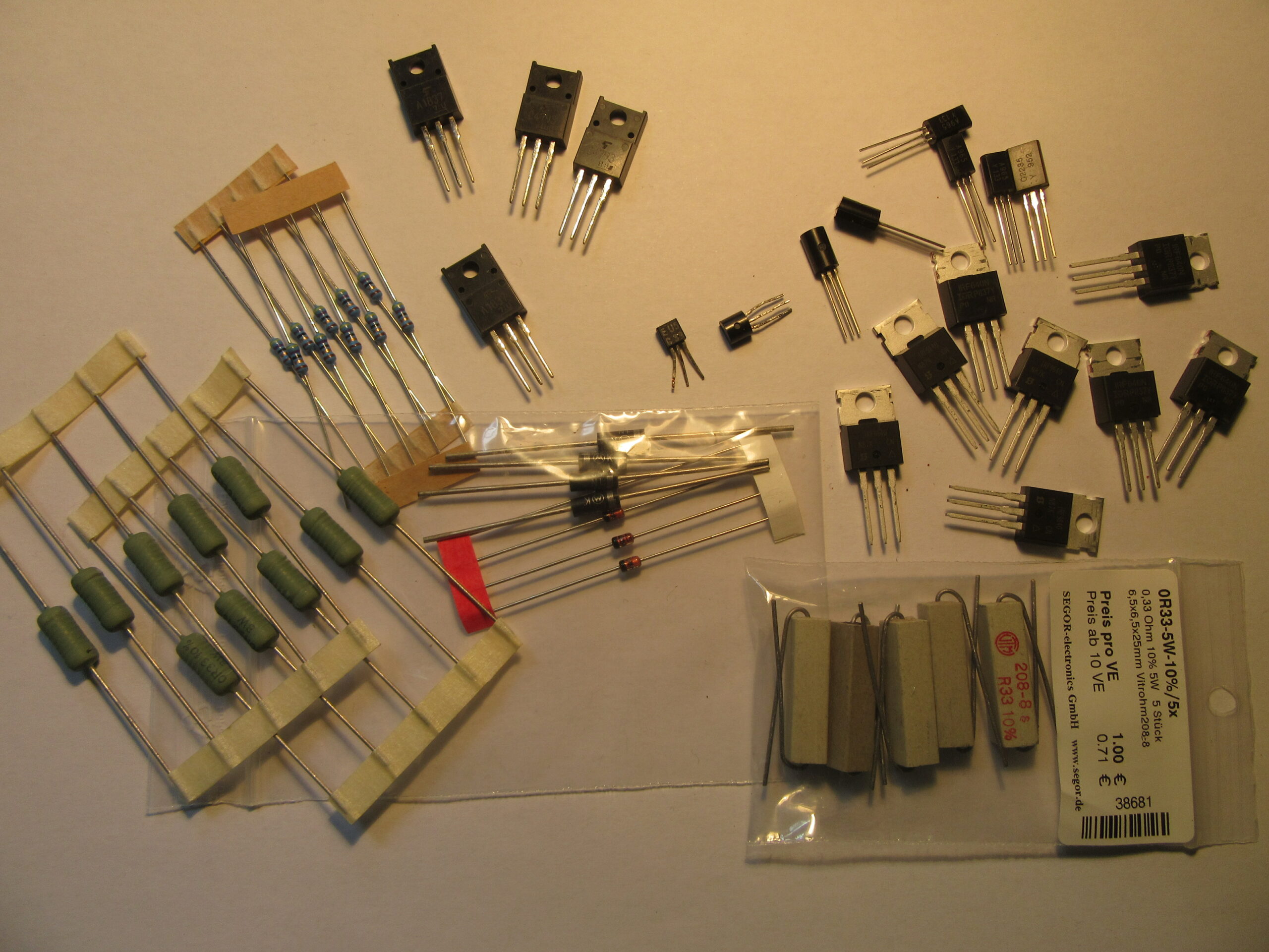
Getting a replacement was easy this time. My local electronics parts dealer SEGOR-electronics GmbH Berlin had everything ready, even relatively exotic Japanese transistors 2SC… were available from stock. However, I had bought the last pieces of a discontinued type.
Spares
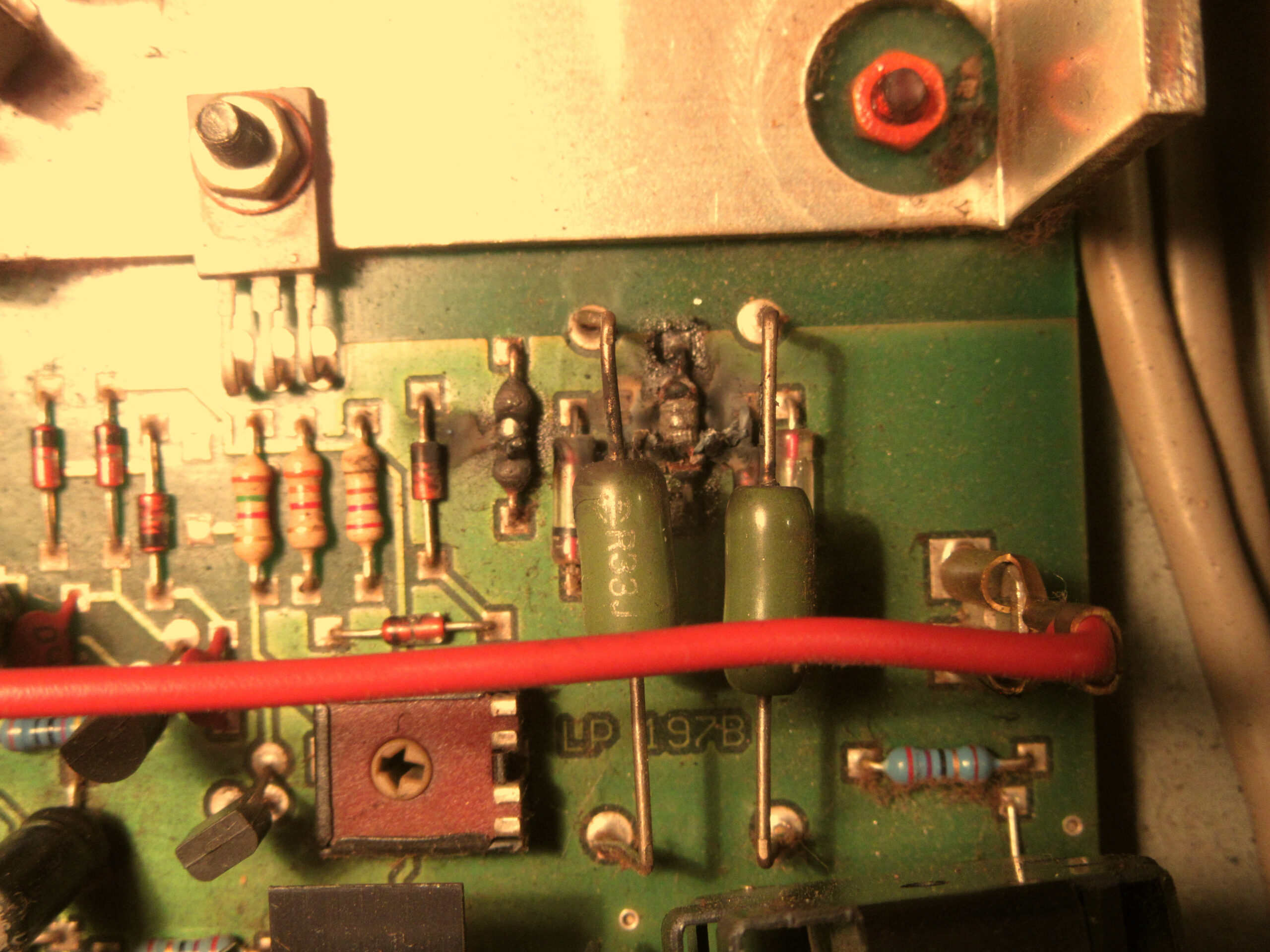
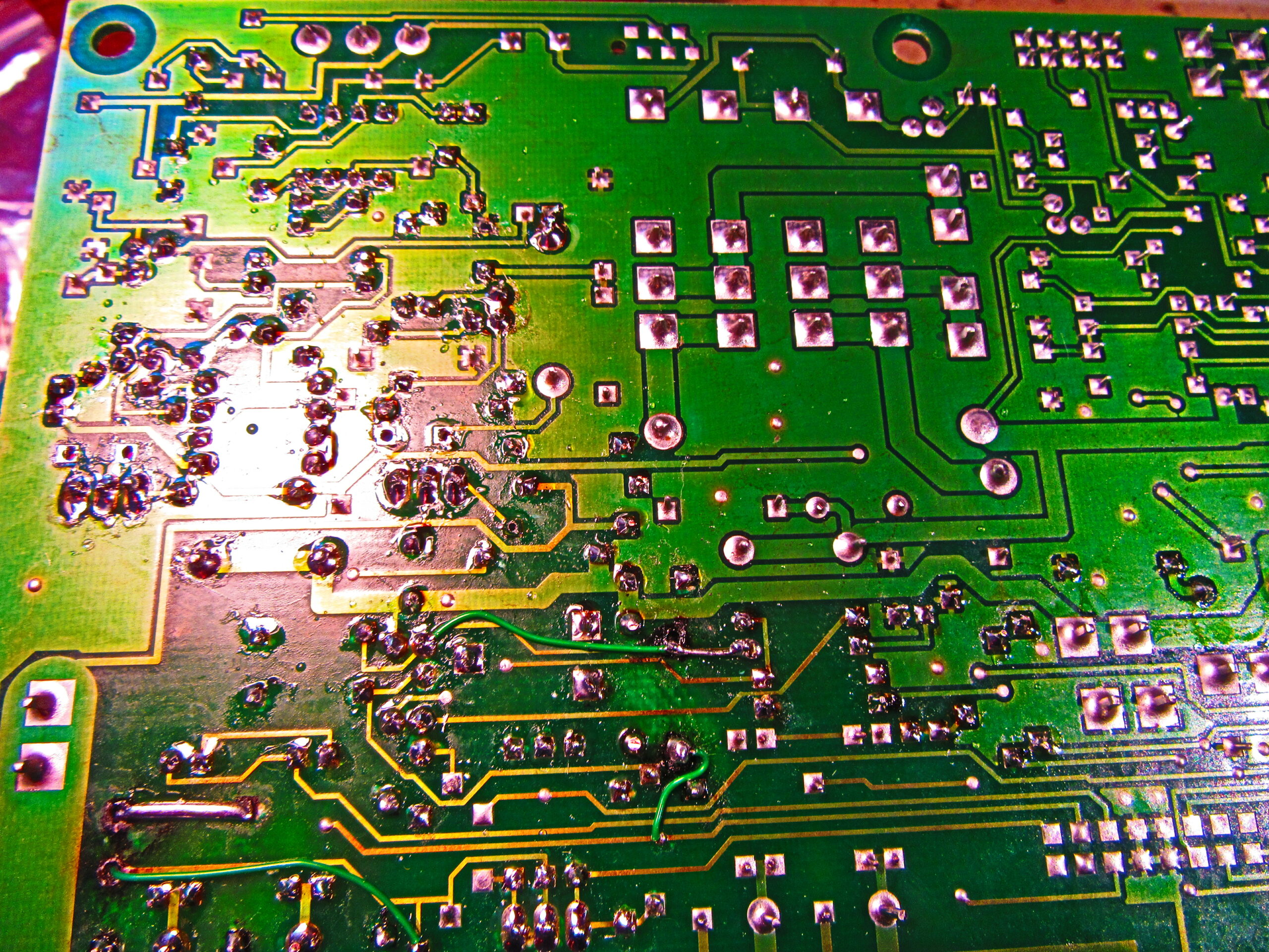
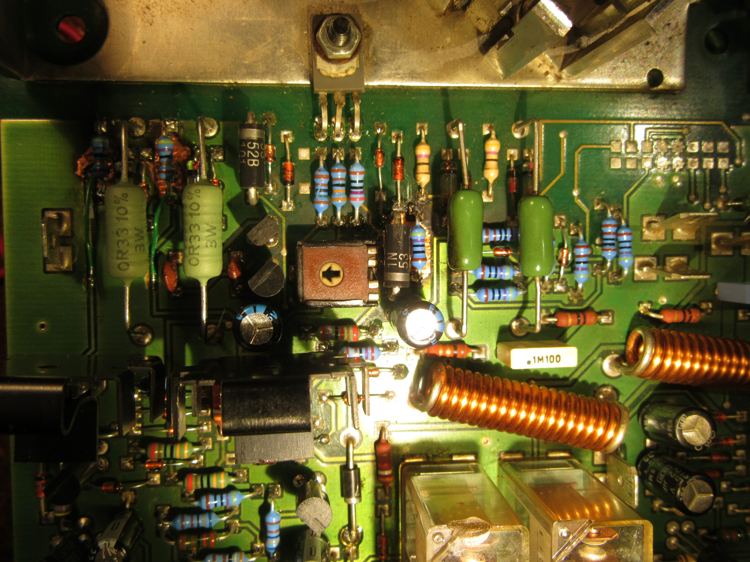
Replacing the parts was not difficult thanks to the circuit diagram and assembly plan. After a few hours everything was done and the vaporized traces were replaced by thin PTFE-insulated wires.
Replaced tracks
Test with precautions
Next up was a first test. This is a delicate matter. If you’ve made a mistake or haven’t found the cause, it goes boom, little clouds rise, and you can swap various parts again. A very good insurance against a new disaster is an upstream bulb. This is looped into the power supply so that the maximum power is greatly reduced and in the event of a short circuit, for example, only the bulb lights up and nothing explodes. For a power amplifier of this size a 100W incandescent lamp is appropriate, good who still owns such a thing.
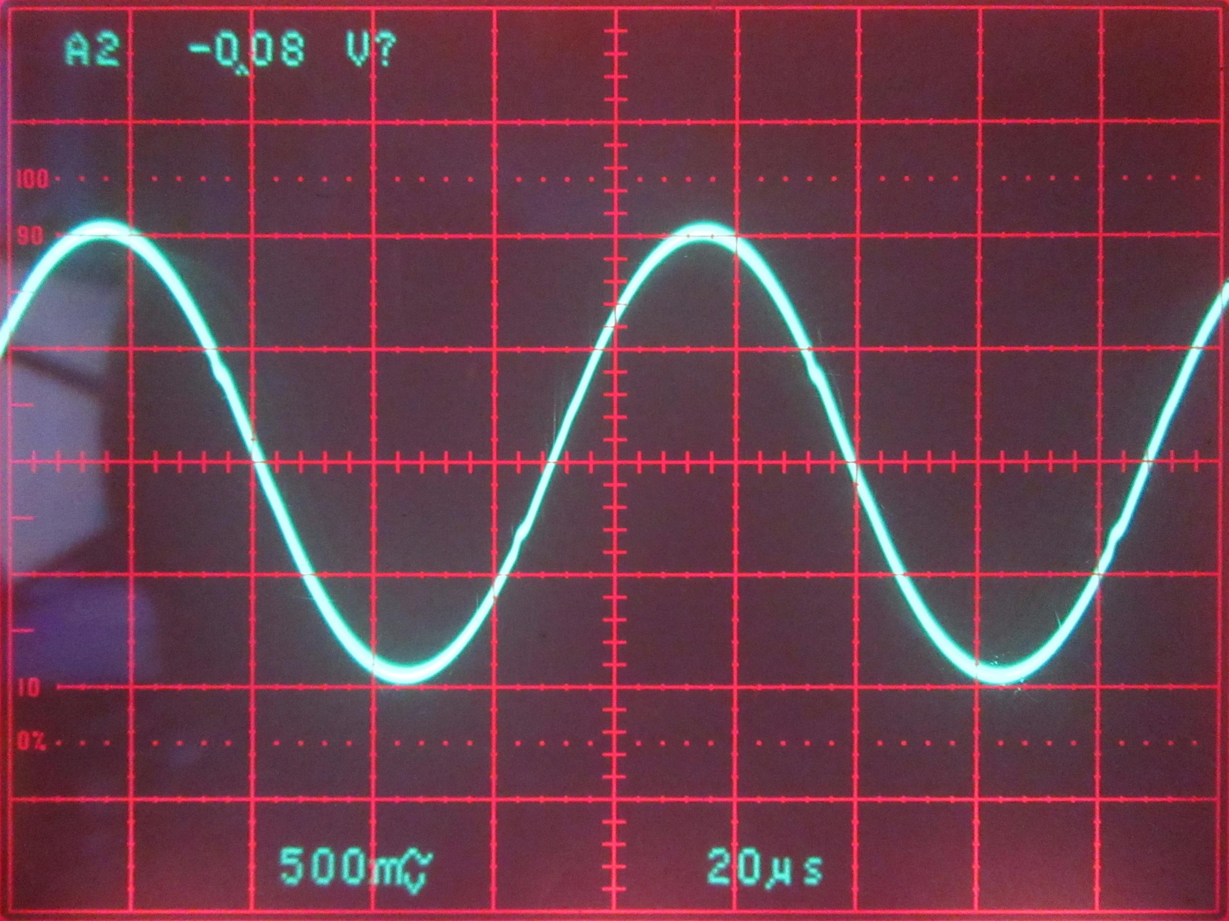
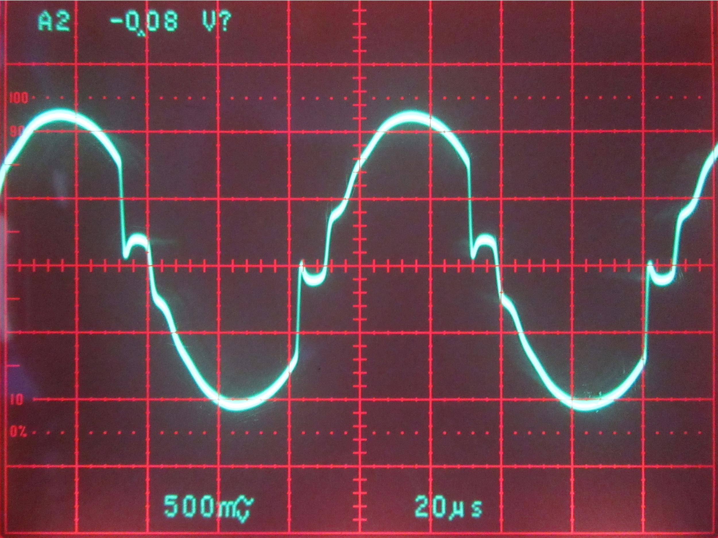
The test went well at first, the fed sinus signal could be seen at the output. However, strong distortions appeared at a slightly higher output level. The unrepaired channel still ran flawlessly.
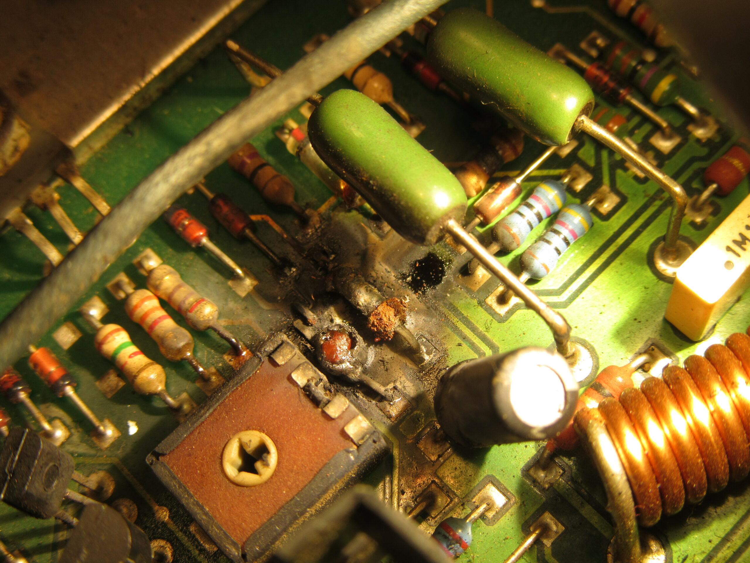
I can briefly summarize the rest of the story. During the repair of the PCB traces I had made a small mistake and connected the drivers of one half-wave with the end transistors of the other half-wave. At low volume the signal was ok, but when the end transistors take over as well, only muck comes out of the speaker. The problem haunted me for a few days. In desperation I changed almost all parts of the defective channel, without success. The unsoldered parts soon resulted in a kind of wimmelpicture.
Replaced sundriesNew components soldered
After sleeping on it for a few nights, I systematically searched for the problem again. Great satisfaction when I found the tiny error and fixed it. Actually, I had done everything else right in the first attempt. That doesn’t work out very often with an extensive repair.
Adjustment
The only necessary adjustment is the quiescent current. For this I simply measured the voltage drop across the drain resistors of the intact channel and adjusted the other channel in the same way.
Error cause and update
In the test run, it turned out that the heat sinks get quite hot even without load. The built-in fans are activated at a certain temperature. The idle temperature seemed too high to me. This also matched a change or an update of the device that was in the documents K.M.E. had sent me. The update causes the fans to run permanently at low speed to prevent overheating. So now I think the cause of the defect has been found. It’s pretty sure that one of the end transistors died of heat and dragged several other components with it.
The update consisting of a 220nF capacitor and two 5.6V Z-diodes was quickly installed.
Finally, only the old, out-of-round and quite loud fans were disturbing, which are now permanently on. The quietest suitable model for replacement was quickly found and ordered.
New fan
The last official act was the replacement of the three fans.
First, I have to justify myself to anyone who asks, “Why the heck is he writing in such detail about restoring capacitors?”
From my point of view, the two most common problems that cause old devices to give up the ghost are primarily defective capacitors and, in second place, corroded contacts of mechanical components such as switches, relays or potentiometers. I will certainly write an article on the latter this year. The capacitors, in particular the electrolytic capacitors (short: elko) I dedicate myself here. Some time ago I started an experiment with paper capacitors, which is still running. The other two common capacitor types – ceramic and film capacitors – are much more durable than those with paper or electrolyte, which is why I have to replace them only in very rare cases and do not report about them here.
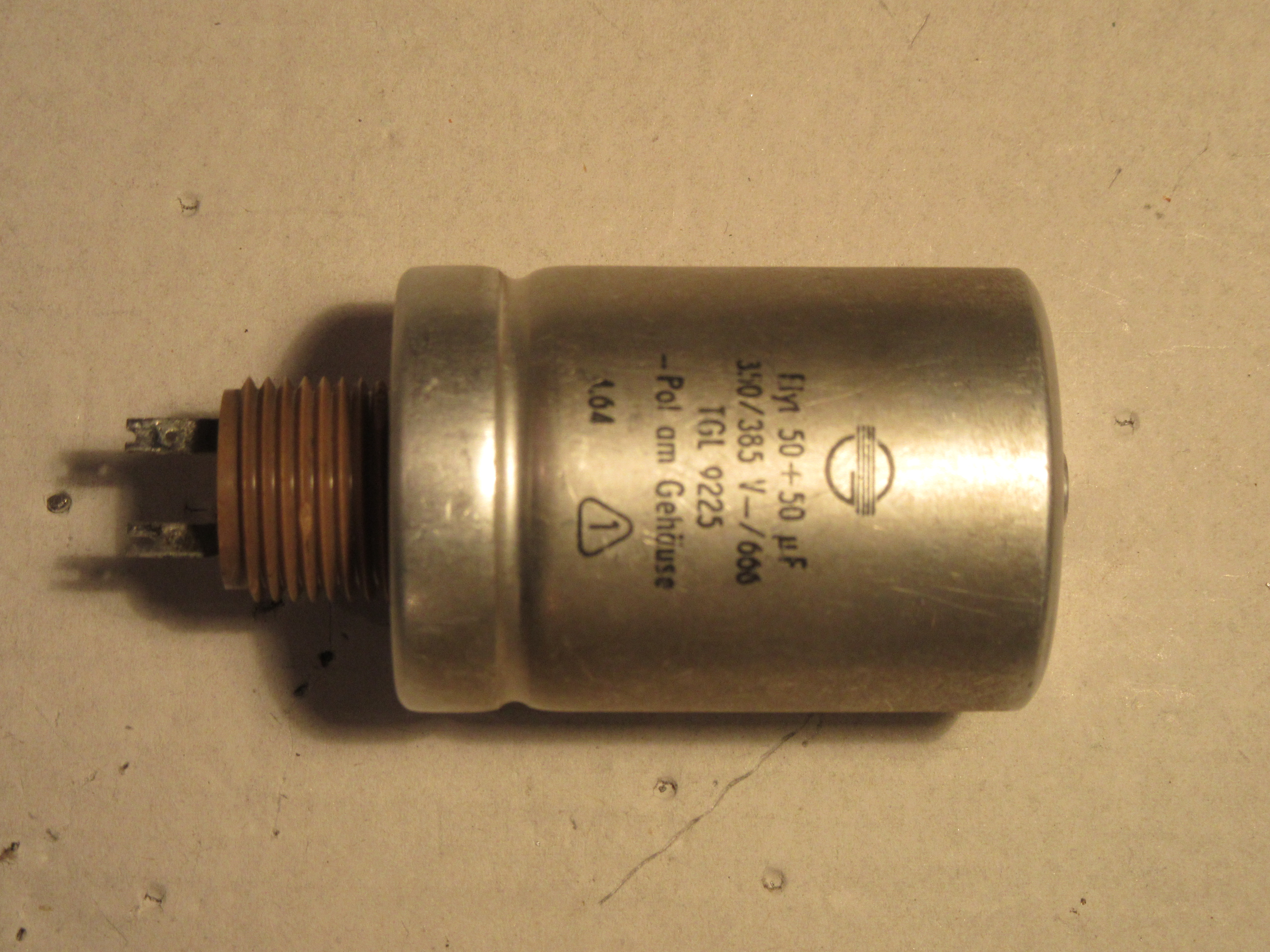
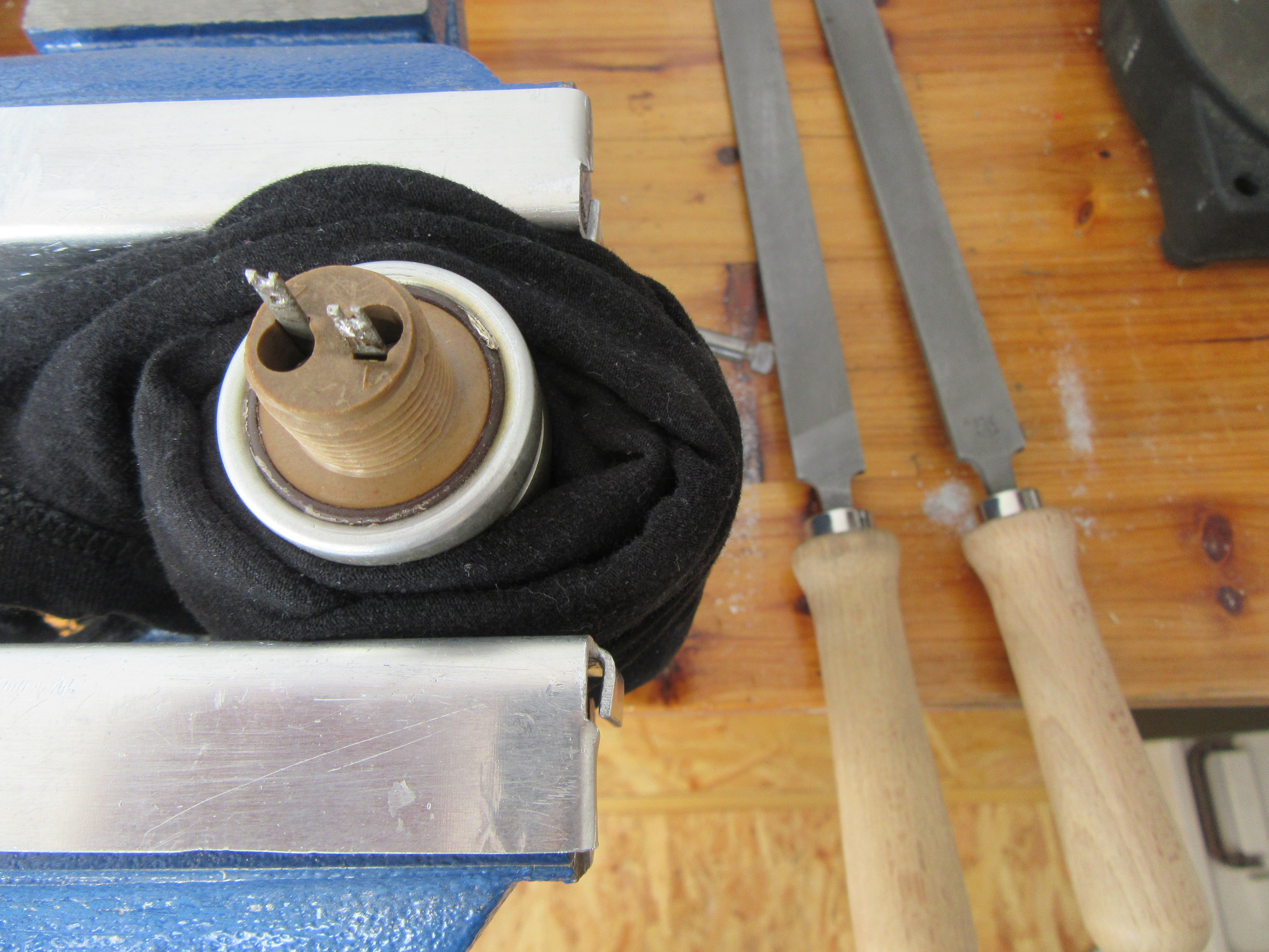
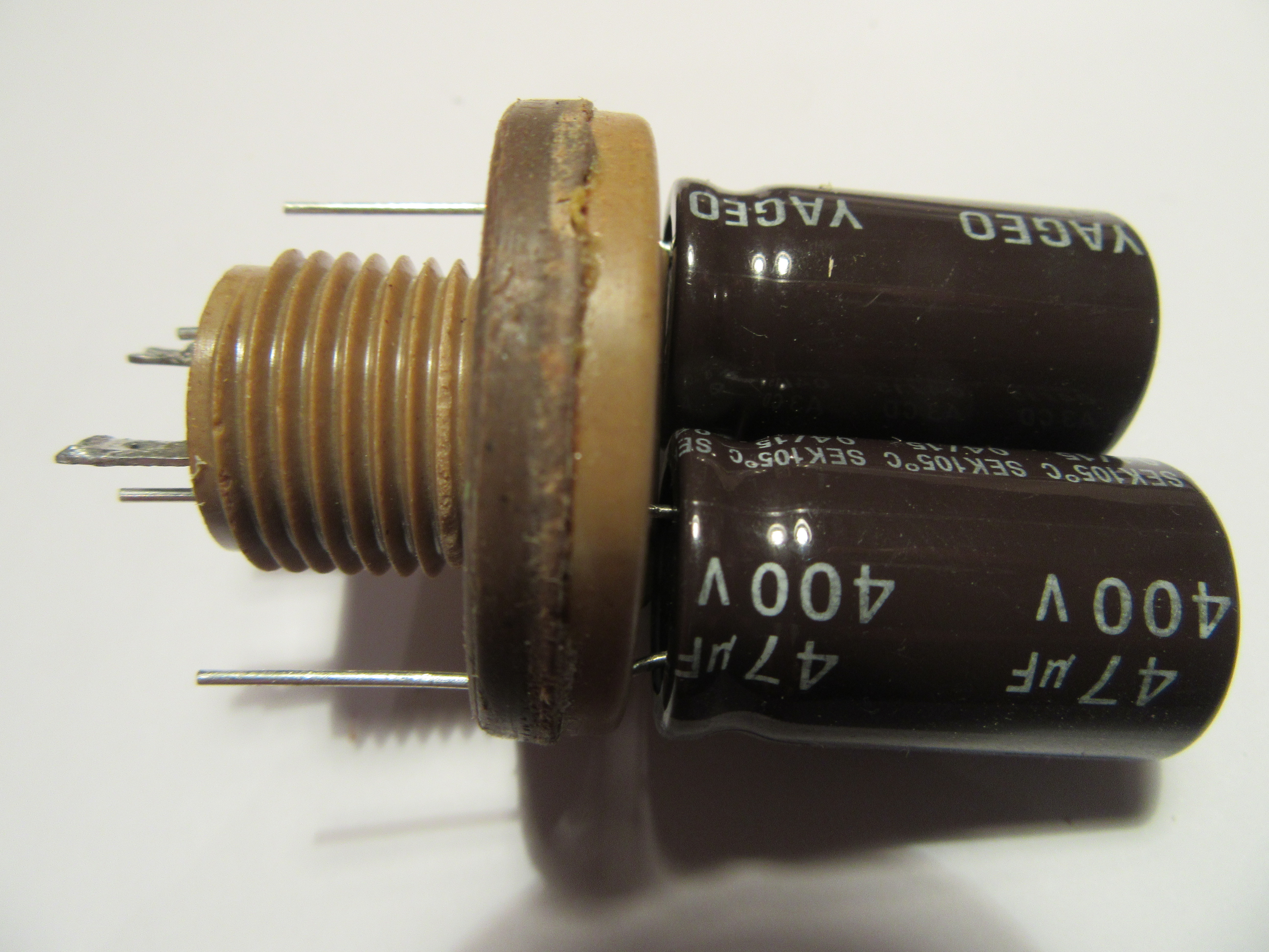
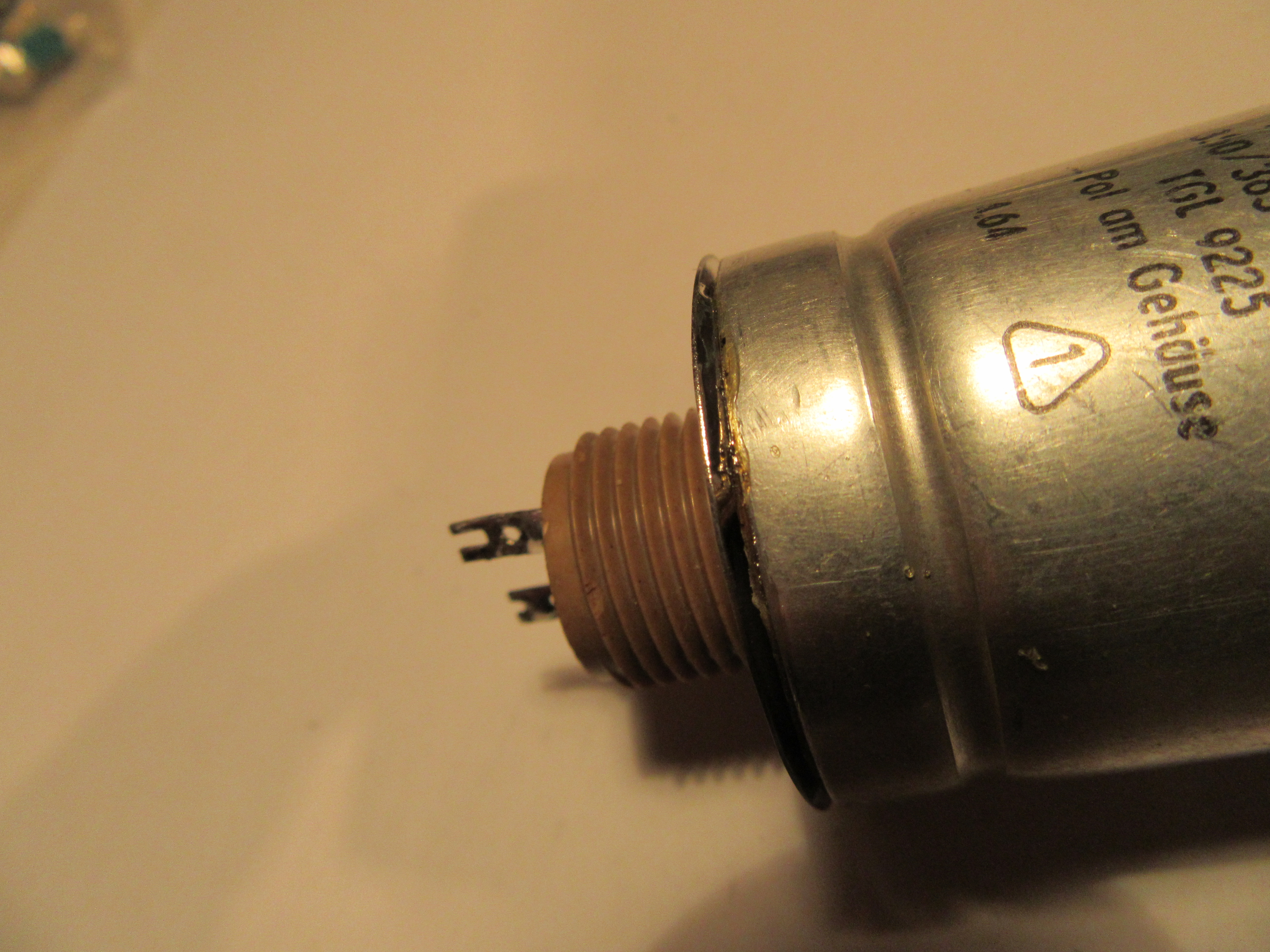
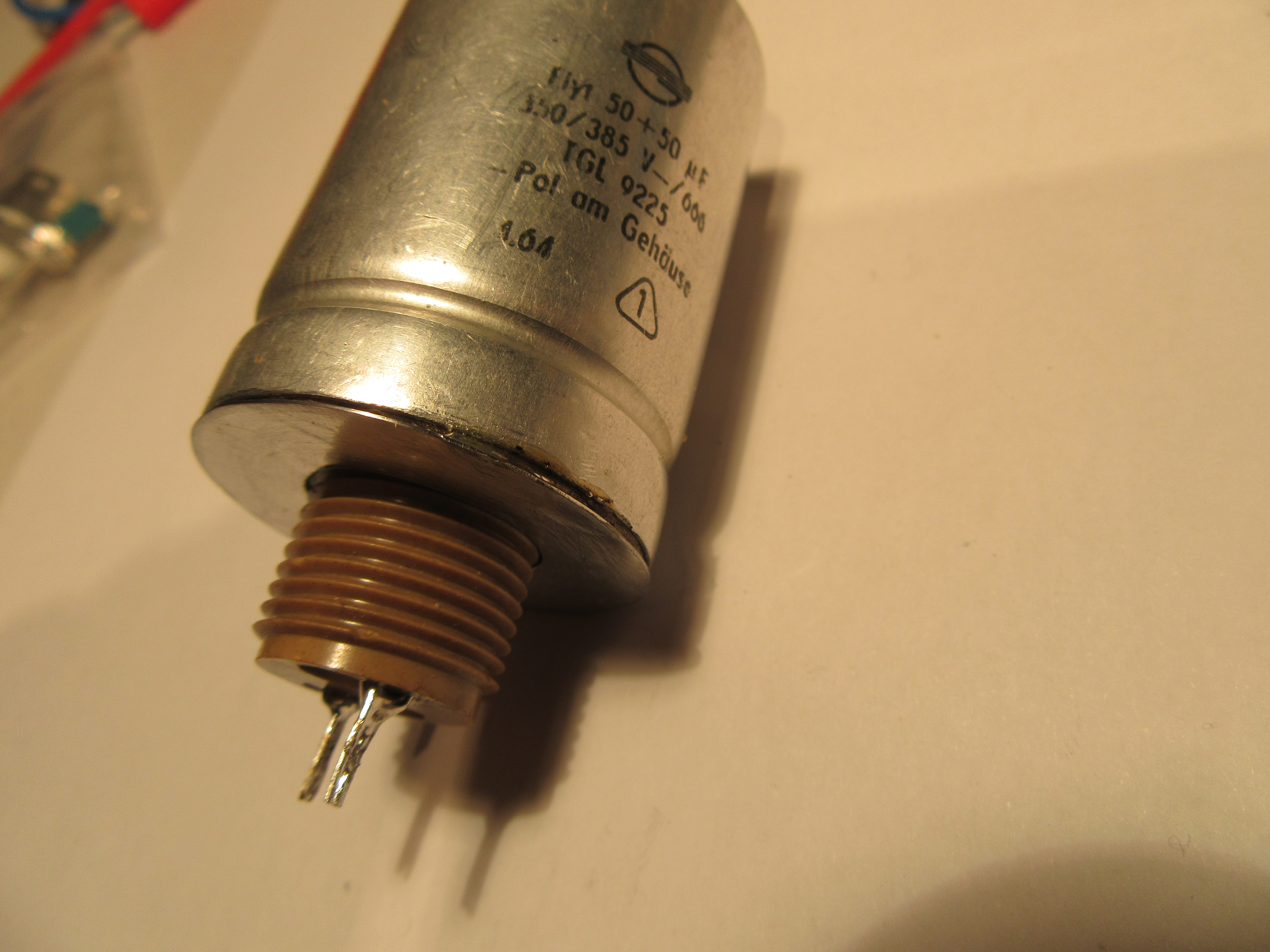
The protagonist of this article is a 50+50µF/350V power supply electrolytic capacitor from a tube radio “Saalburg 5170” from VEB Stern-Radio Sonneberg, which I had repaired for my friend Axel in early 2015.
The corpus delicti
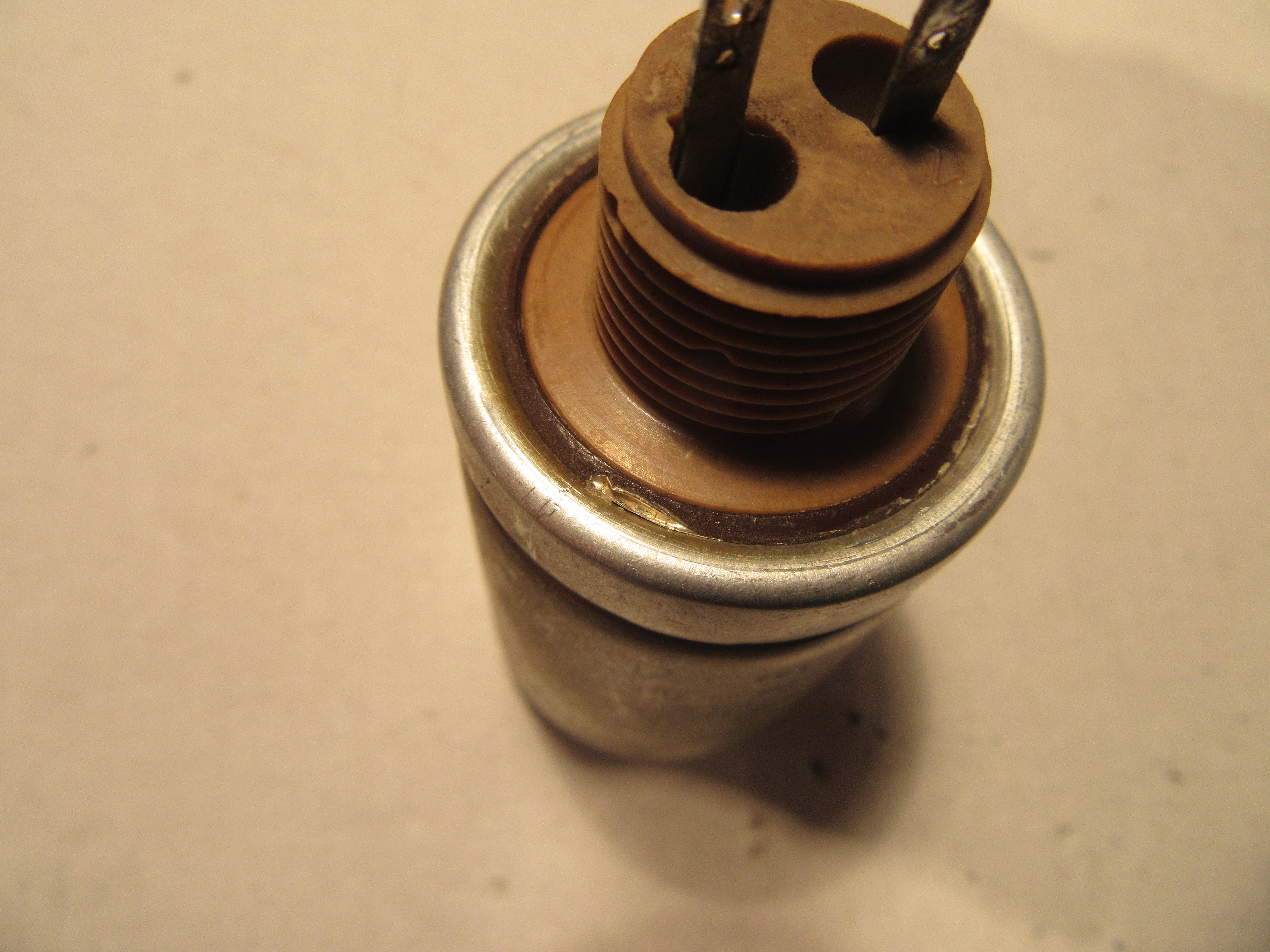
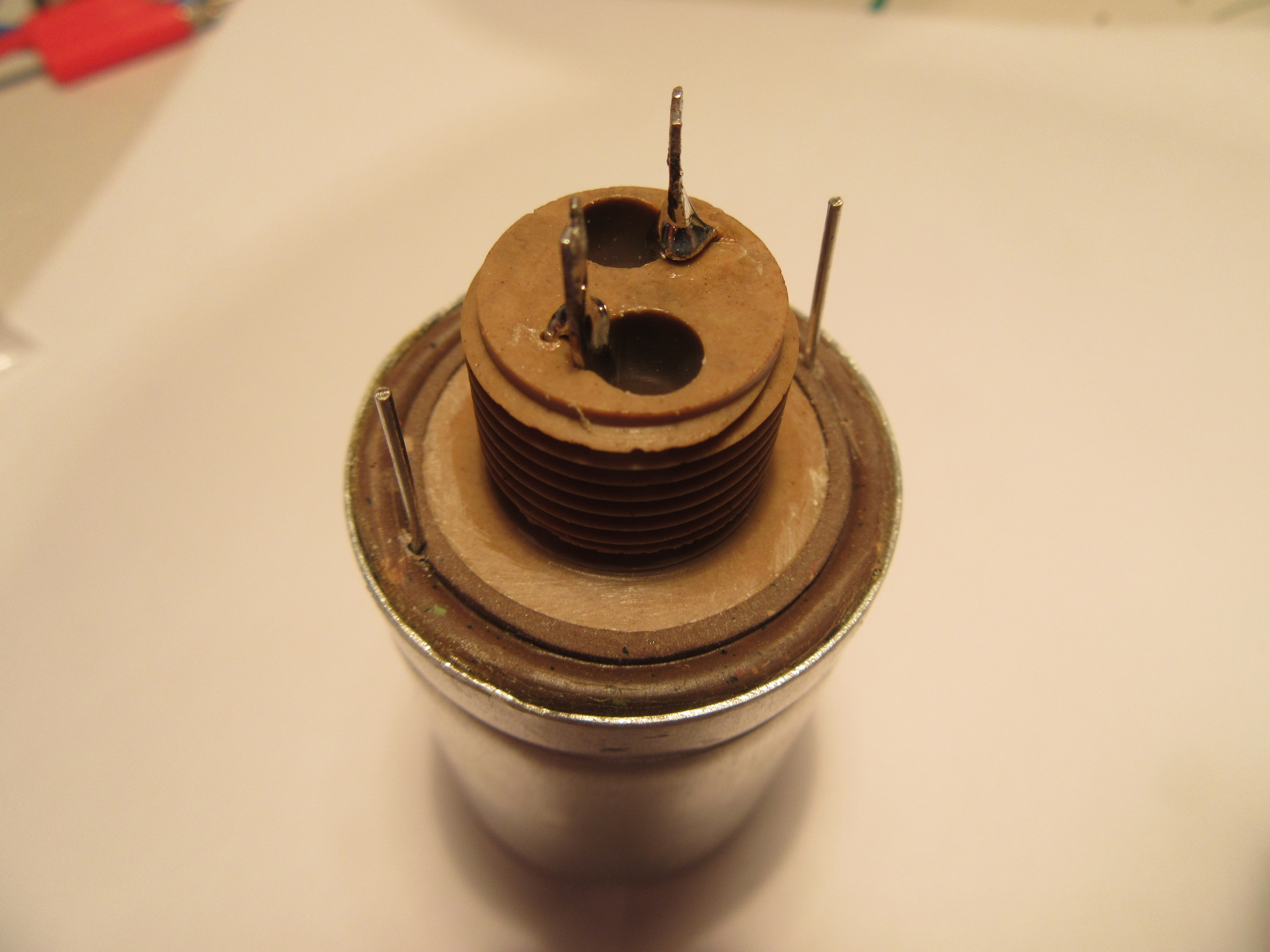
The radio must have been humming since we bought it, and in fact we found a manufacturing defect that is now being fixed after 50 years. The capacitor was not flanged correctly, so the electrolyte leaked.
Visible defect on the flanged edge
Structure of electrolytic capacitors
But now to the topic. I can’t summarize what you need to know better than Wikipedia.
The most important point is that it is an aluminum foil, which has a thin oxide layer on one side. The whole winding is in a liquid, the electrolyte. This ensures that the oxide layer is formed in an electrochemical process. An electric field or voltage is necessary for this. The process of building up the oxide layer is called forming. Another important term is leakage current, which refers to the current that passes through this oxide layer, so to speak. The lower the leakage current, the better. The higher the current, the more power loss we have in the capacitor, which can lead to heat generation and, in extreme cases, even explosion.
Defects
The three most common defects are:
Degradation of the oxide layer after a long period without operation
Leakage of the electrolyte or drying out
Short circuit or breakdown
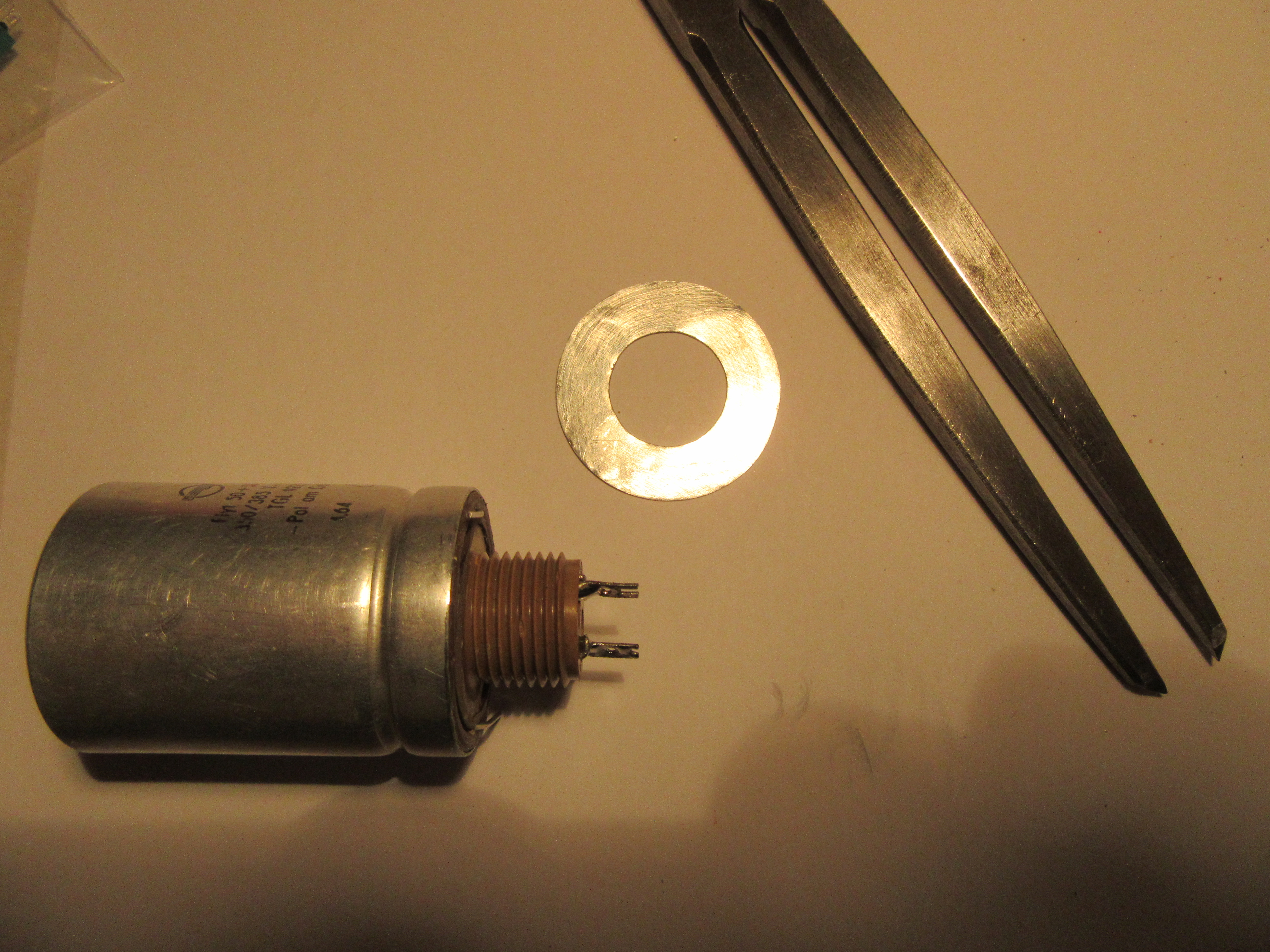
In the case of point one, the capacitor can be reformed. In the case of points two and three, the component is lost. But you can save the case and replace the inner part with a capacitor of current design. This way it is at least possible to preserve the outer appearance and the function, which is an important point for restorations.
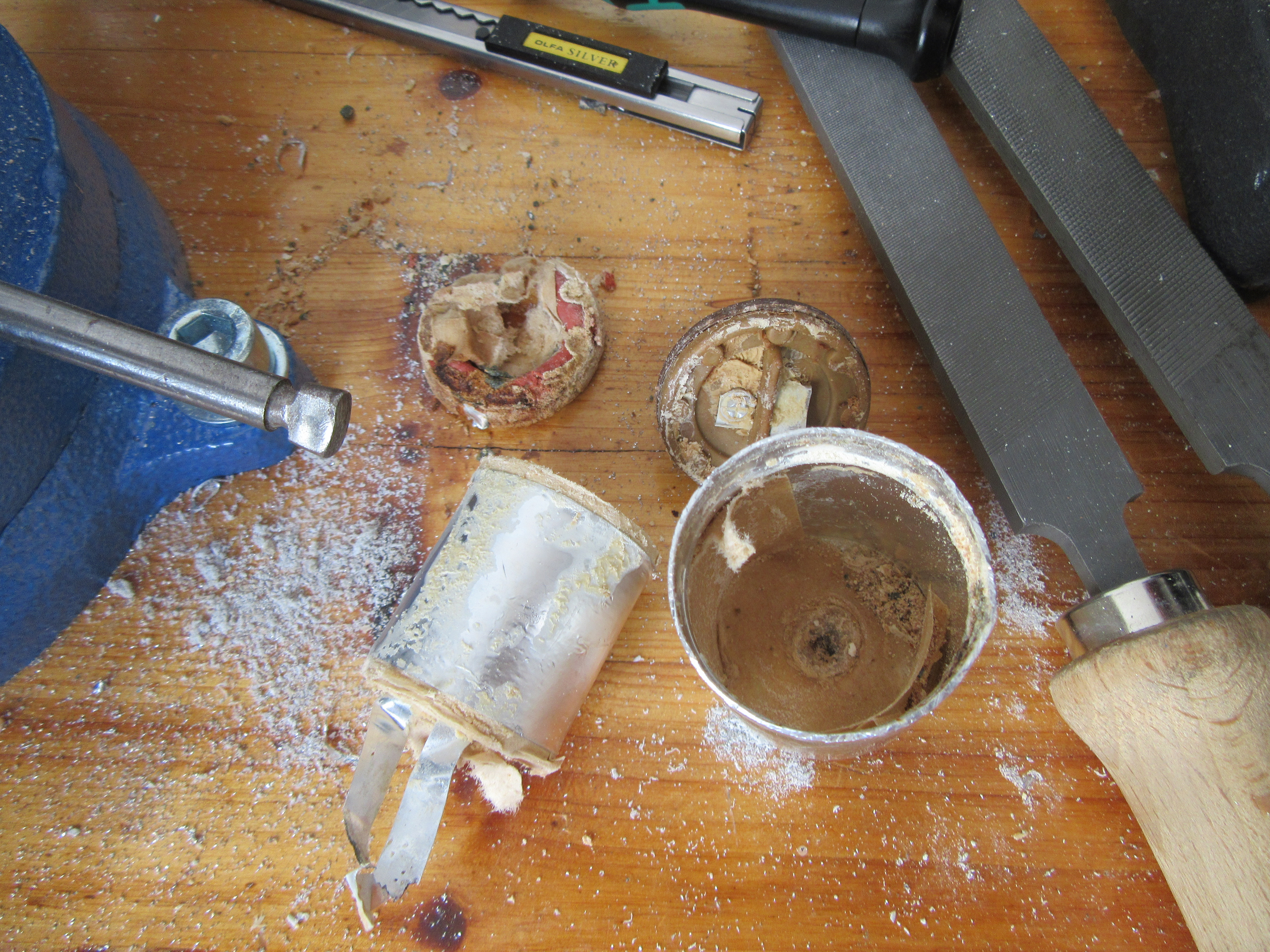
Open electrolytic capacitor and replace inside
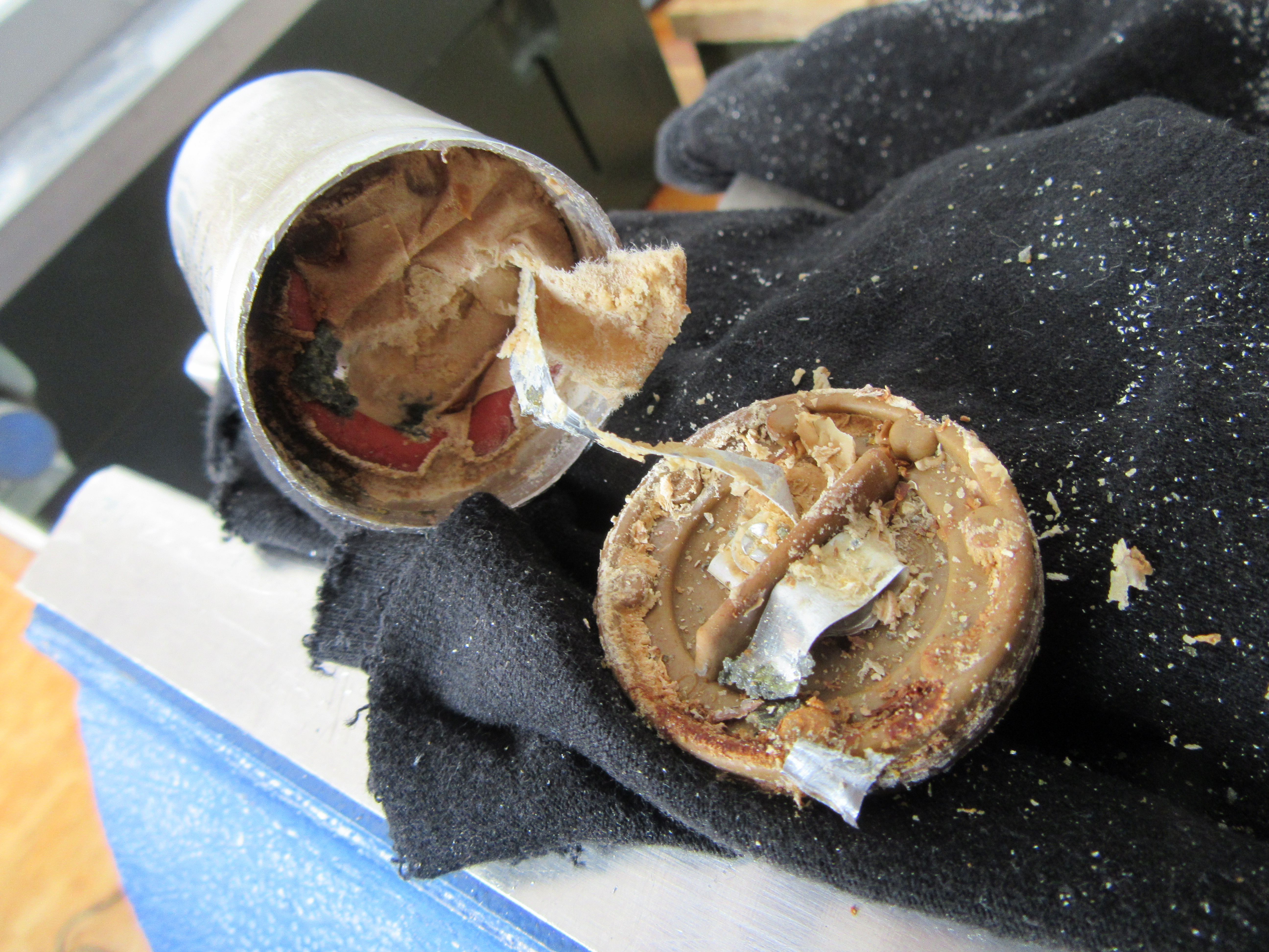
I present this process here as a small picture story. In fact, the electrolytic capacitor was as dry as dust inside as suspected. As a safety note, I would like to add that gloves and a respirator should be worn for the work. Normally, the electrolytes from standard electrolytic capacitors are non-toxic, but whether in the 50s and 60s really value was placed on non-toxicity, I dare to doubt.
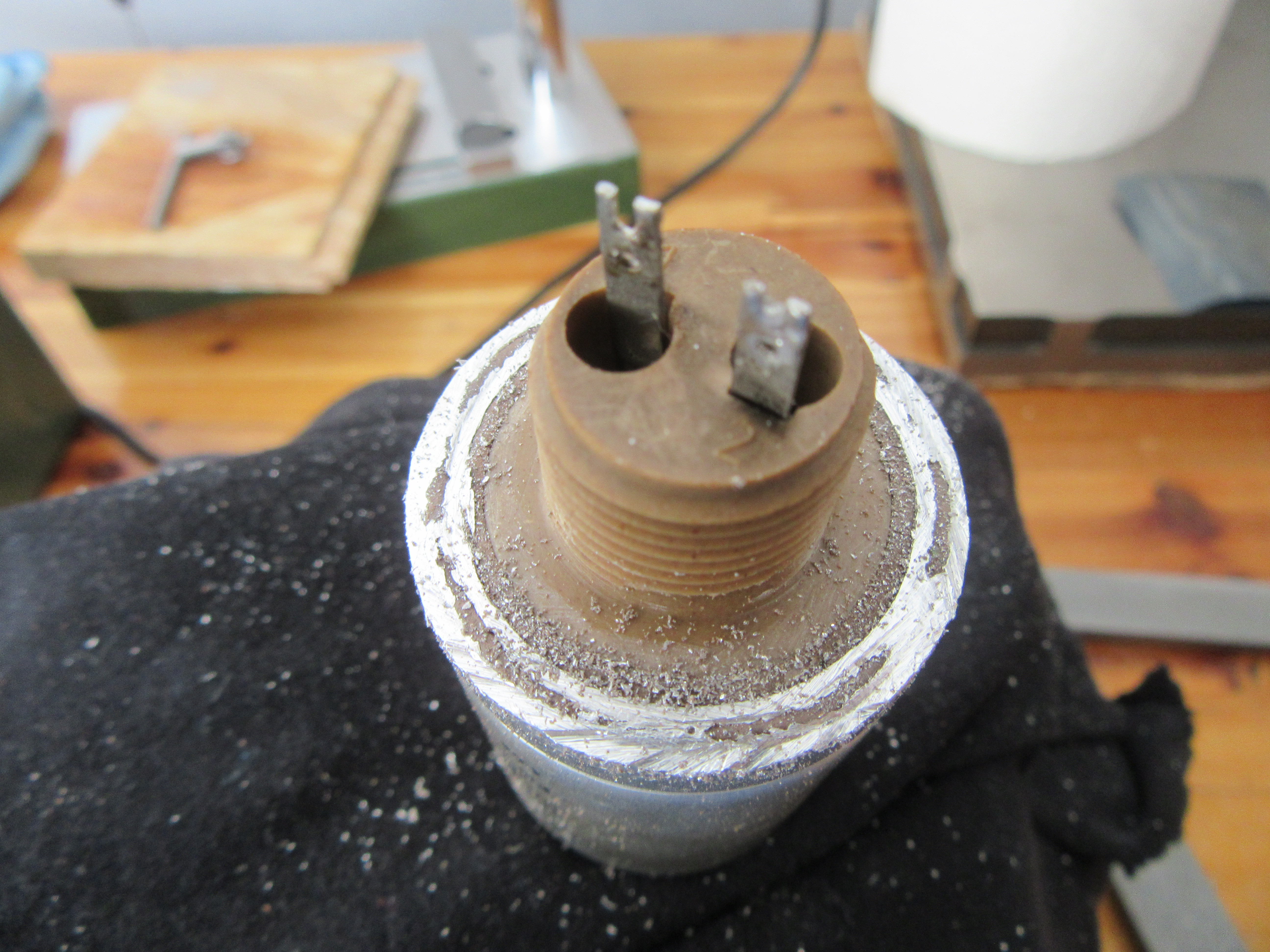
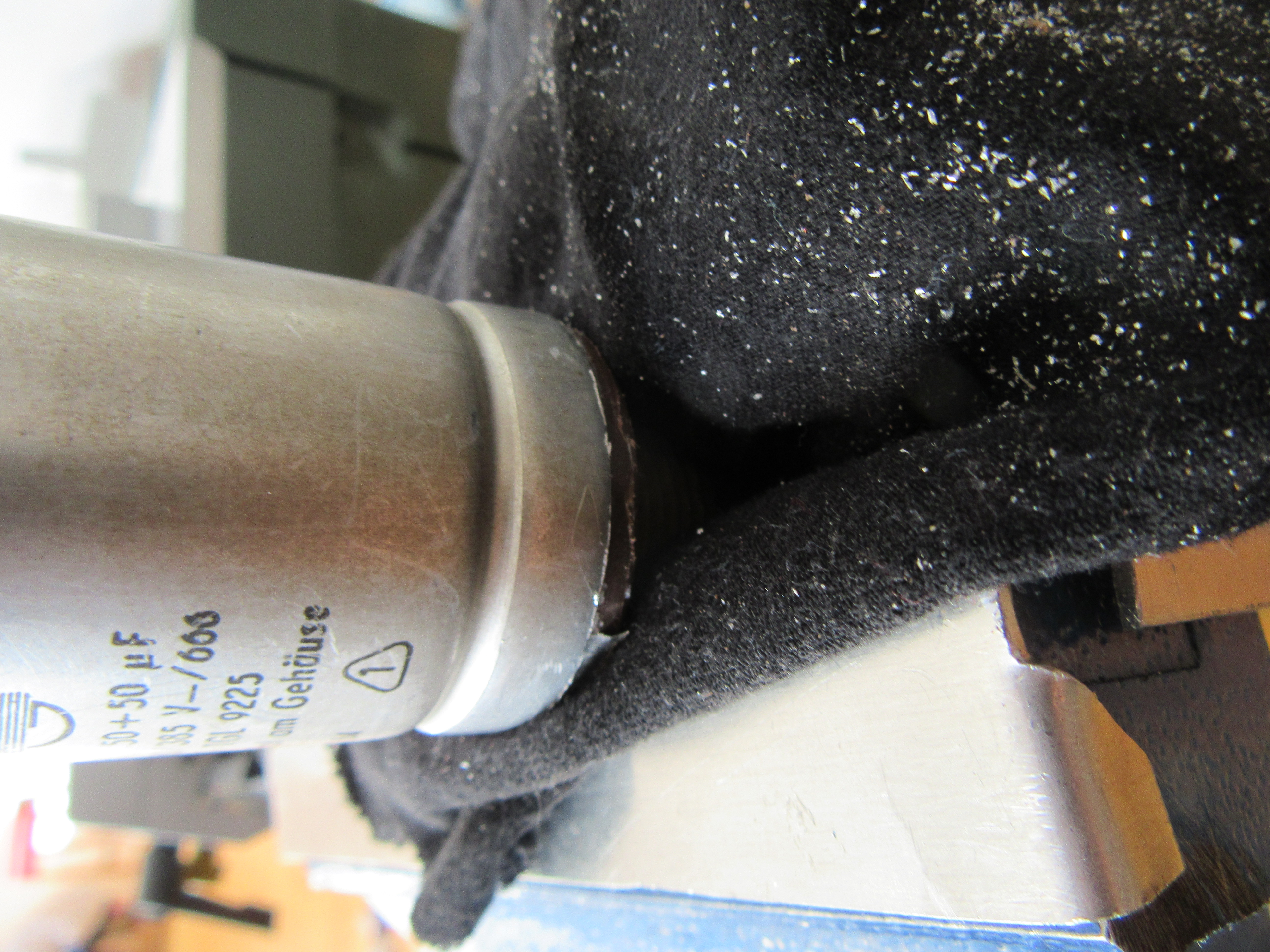
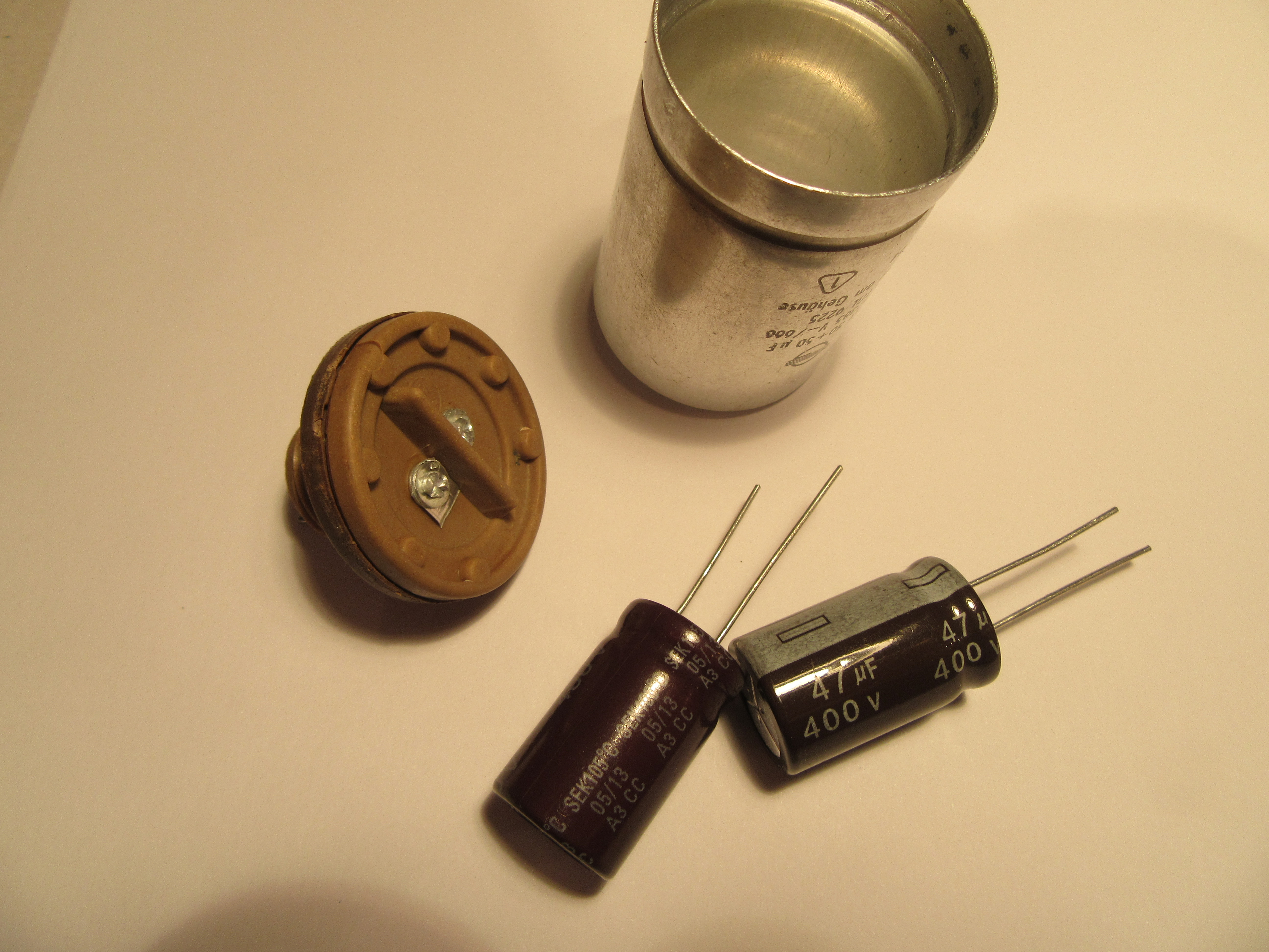
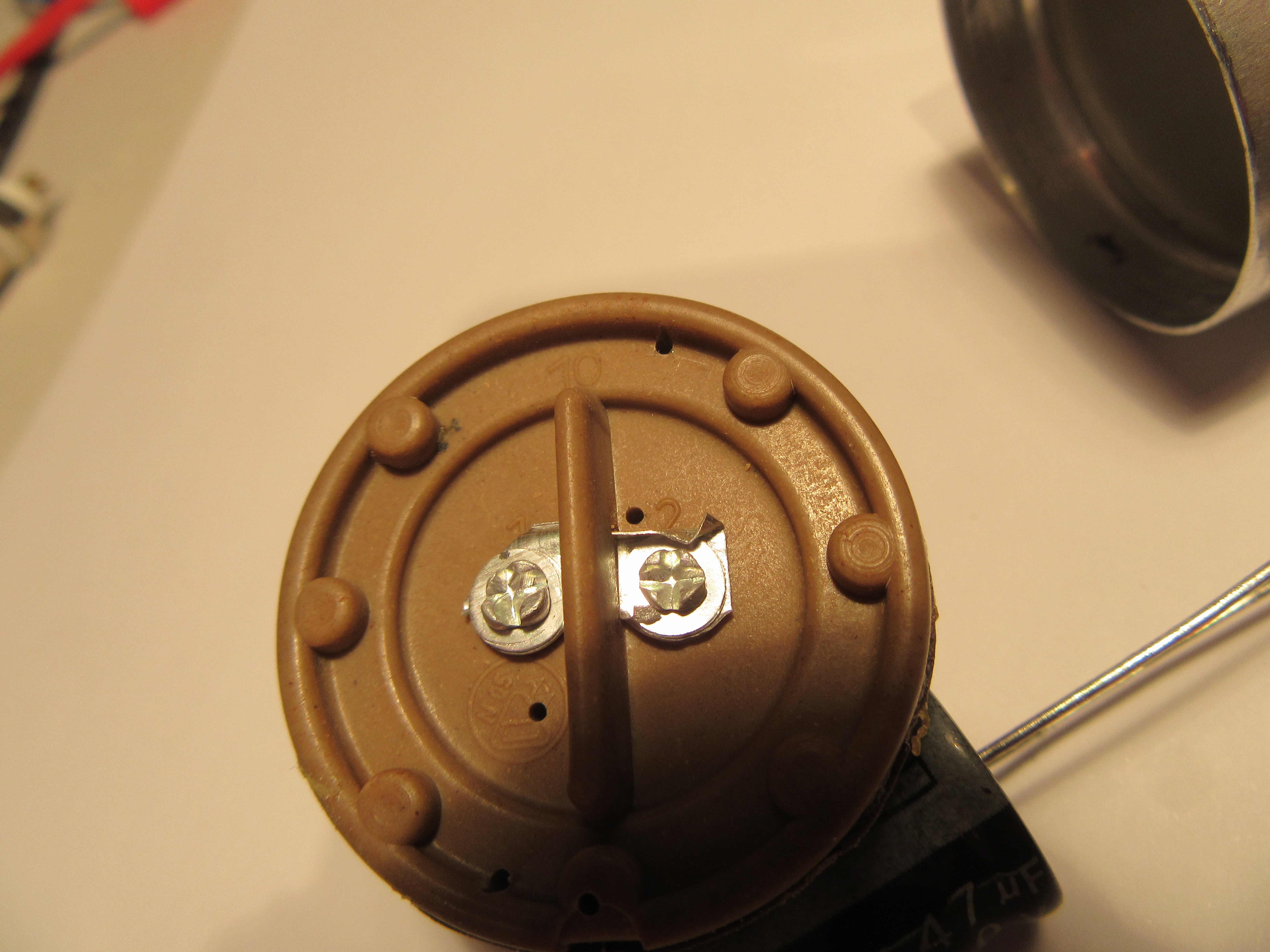
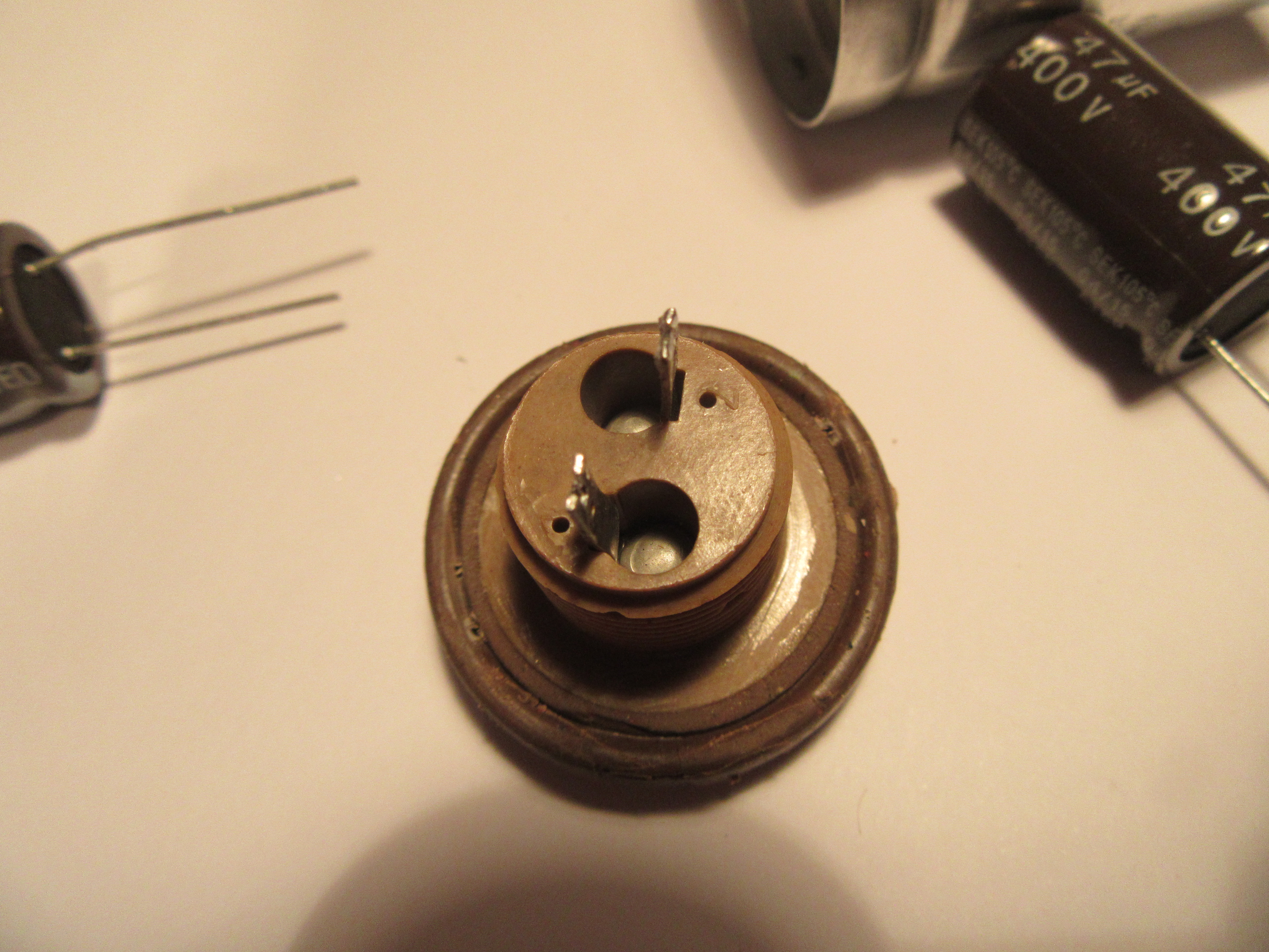
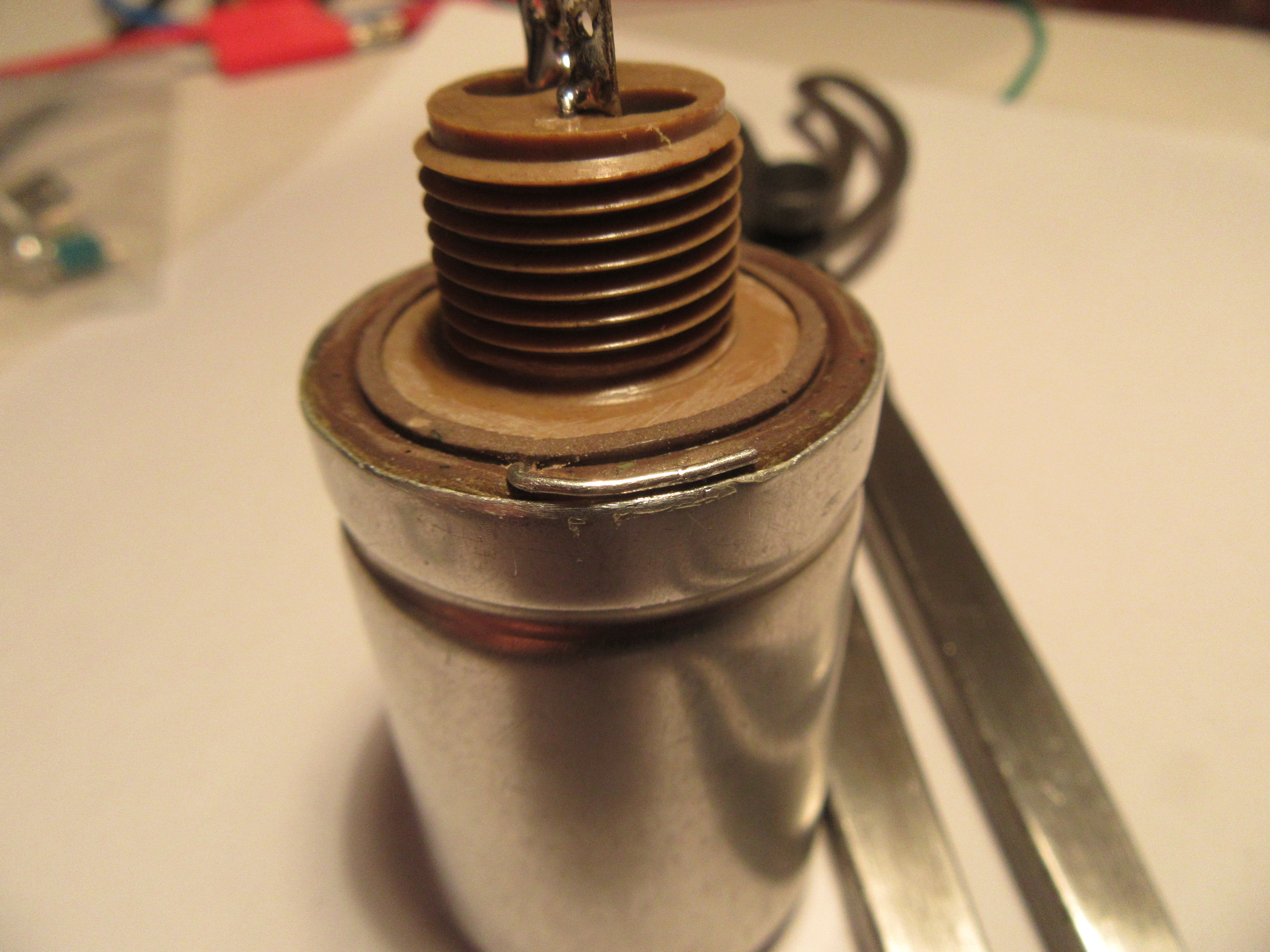
Wrap in a cloth and carefully clamp in the vice, do not dent it!File off the edge with a fileClamp with the thread and pull off the cup upwardsFoot is removed, the wrap is still in the cupIf the wrap is stuck, it can be removed with a large screwCup and foot are cleaned with a toothbrush and scouring milk, the replacement capacitors are ready4 holes are drilled in the base, diameter 1mm for the connections of the new electrolytic capacitorsThe positive poles are placed directly next to the old terminal lugs, the negative poles in the outer ringInstallation of the replacement electrolytic capacitorsThe positive poles are placed around the old terminal lugs and soldered, the base or the rubber sealing ring is glued to the cup with PattexThe new negative pole is made from a disc of tinplate, inner diameter 18mm, outer diameter about the electrolytic capacitor thicknessThe two negative poles are bent overThe tin plate is soldered to the two negative polesReady and operational for another 50 years, even experts can hardly tell the difference
Elko reform
In general, devices with a mains connection that have not been switched on for a very long time should not be put back into operation so easily. Often the power supply electrolytic capacitor then causes a short circuit, which leads to various subsequent errors. The electrolytic capacitor must be reformed, for which there are two basic possibilities. You can do this in the device or you can remove the capacitor.
Reform in the device
If someone uses the procedure described here himself, then expressly at your own risk. I have already done this several times with success, but that does not mean that it always works. The procedure is simple and relies on the fact that old devices are quite robust and a short circuit does not harm the power supply. Every day, the power is turned on a little longer. After that there is a resting period in which the oxide layer in the electrolytic capacitor can build up again.
day 1: Switch on for 5s
days 2-3: Switch on for 10s each
days 4-7: switch on for 20s each
from day 8: double the time every day
For very old devices, i.e. older than 50 years and for particularly careful procedures, the phase days 2-3 must be extended to considerably more days, I would suggest up to 2 weeks.
Reforming with high voltage power supply
My preferred method is forming with a high voltage power supply with current limiting. This is a very safe method if you monitor the leakage current and slowly increase the voltage accordingly. The duration of the process goes from a few hours to several weeks. It depends entirely on the age and design of the capacitor. The voltage is slowly increased while taking care not to exceed the maximum leakage current.
My guideline values for the maximum leakage current are:
50µA per µF for 350V capacitors
100µA per µF for 500V types
For capacitors that are from the 40’s or early 50’s, the leakage current can go as high as three times that value. The important thing is that at some point a stable value is established.
Of course, a high voltage power supply and a current meter with 1mA measuring range is not available to everyone. Here I have found a tutorial, how it is also easier: