DS1250Y/DS1650Y FRAM Replacement

Abbildung, erster Prototyp im Programmiergerät

This project is not very big but still something special. On the one hand it is part of a restoration which has been prepared for years. On the other hand it seems that nobody has come up with the idea to replace a 5V NVRAM with a 3.3V FRAM or to publish it.

Problem components NVRAM

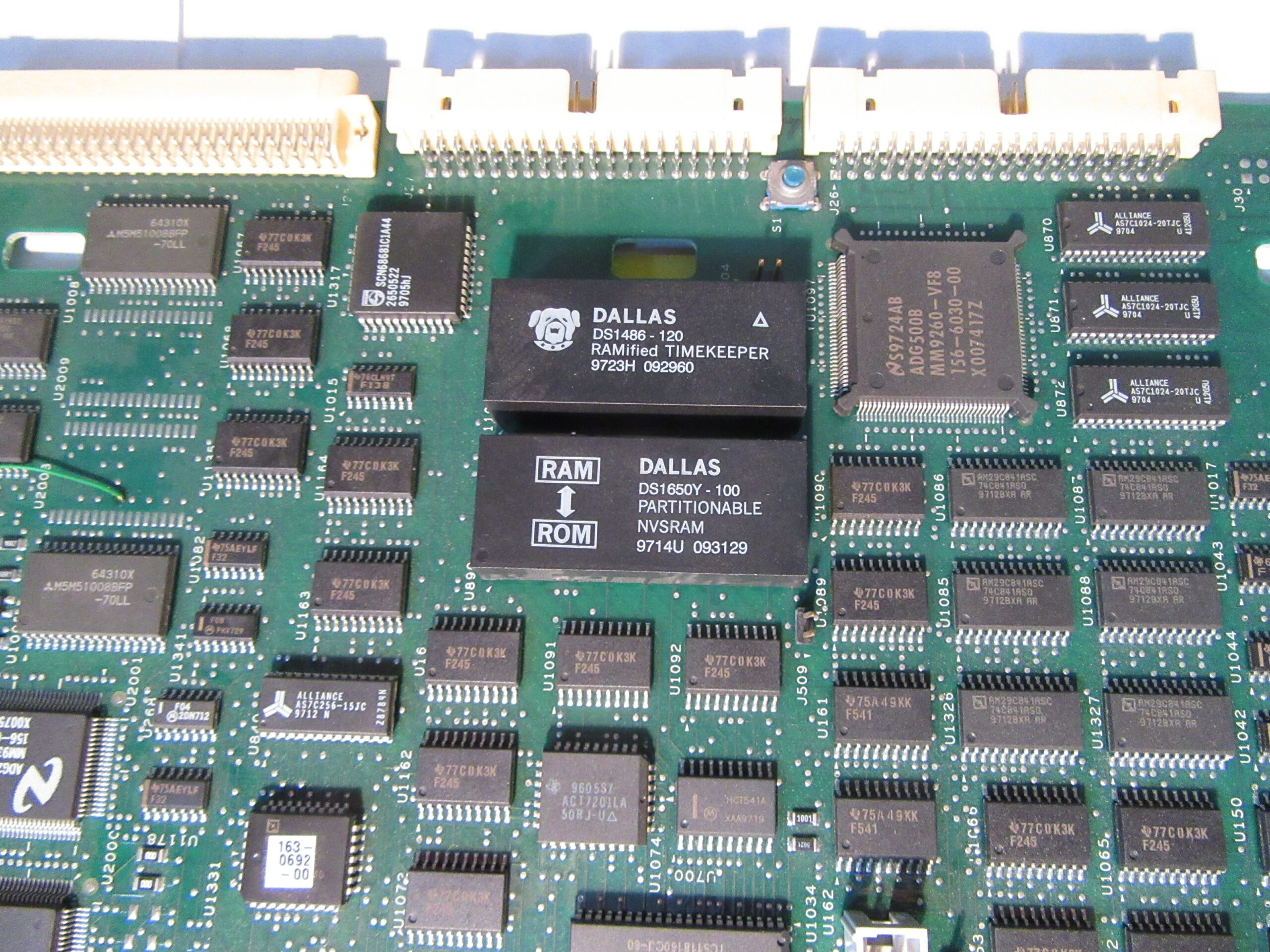
If you want to keep old devices for a long time, you will always come across chips with integrated lithium battery from “Dallas Semiconductor”, which was bought by “Maxim Integrated” in 2001, which in turn was bought by “Analog Devices” in 2021. These are mostly NVRAMs (non-volatile RAM) or RTCs (real-time clocks) with NVRAM. The battery integrated in the chip package enables the data in the RAM to be retained even after the operating voltage is switched off and the RTC continues to run. An NVRAM controller, which is also integrated, takes care of switching between battery and operating voltage as well as data protection when switching on and off.

Basically, this is a very practical solution, since one can use a single component instead of a whole circuit including battery. However, it is fatal when the built-in battery is exhausted after about 20 years. Almost always the whole device is no longer functional. The components are of course no longer produced. Also the remaining stock traded on the Internet is either already too old or even more often faked. I have bought two fakes myself. Thus, replacement with the original part is not an option.

Example photo of soldered NVRAM and RTC
Soldered NVRAM and RTC (Tektronix TDS754C CPU Board)

Replacement options

The replacement of RTC and NVRAM differs significantly.

The NVRAM can be replaced by a corresponding SRAM with NVRAM controller and battery. Some examples can be found on the net.

Another variant is the replacement by FRAM, a memory which can be written arbitrarily like RAM, but which keeps the content even without operating voltage. There are also examples with the FRAM types FM16(W)08 and FM18(W)08 with 64kBit and 256kBit size respectively. The charm of this solution is that no battery is necessary and thus the memory remains maintenance-free. Unfortunately, the two mentioned FRAM types are pin-compatible with the Dallas NVRAMs, but they are controlled somewhat differently. Thus the exchange unfortunately does not work in all devices.

An RTC cannot be replaced so easily. The RTC maps the time to a memory area that is accessed like “normal” RAM. The chip has to keep the required timing exactly. This can only be ensured by using dual-port RAM. However, I have not found suitable circuits. This would be a small project for the future. Currently, there is only the possibility to mechanically drill out an old RTC and connect a new lithium battery from the outside. Or you can use a compatible RTC chip, which is still available as residual stock. As far as I know this is only possible for a DS1486, which is replaced by a DS1386G incl. RAM and battery.

DS1250Y/DS1650Y FRAM Replacement

Now to the corpus delicti. The DS1250Y component from “Dallas Semiconductor” is a 4MBit NVRAM. The pin-compatible DS1650Y variant also has the option of write-protecting individual memory areas via software. Thus the DS1650Y can replace the DS1250Y. The other way around, this doesn’t work in every case, but only when the software doesn’t use the write protection feature or doesn’t depend on it.

A short component search for parallel 4MBit FRAM brings only one product to light, the FM22L16-55-TG. Unfortunately, it works with a maximum of 3.3V and has 16 bit data width in contrast to 5V and 8 bit on the DS1250Y.

So there are still some parts missing to adapt the FM22L16: Some logic, level shifter, a voltage regulator and some brain power. Difficult in the design was also that the whole circuit has to fit on a board with the size of the original part.
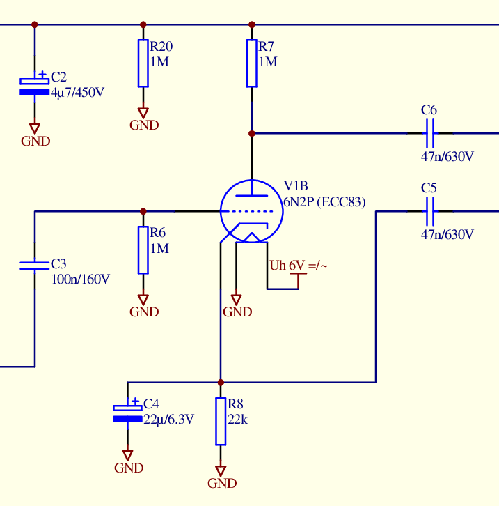
Circuit

After a couple of days of reading and understanding data sheets and drawing schematics, the circuit was ready.

Figure, DS1250 FRAM replacement circuit diagram
Circuit diagram

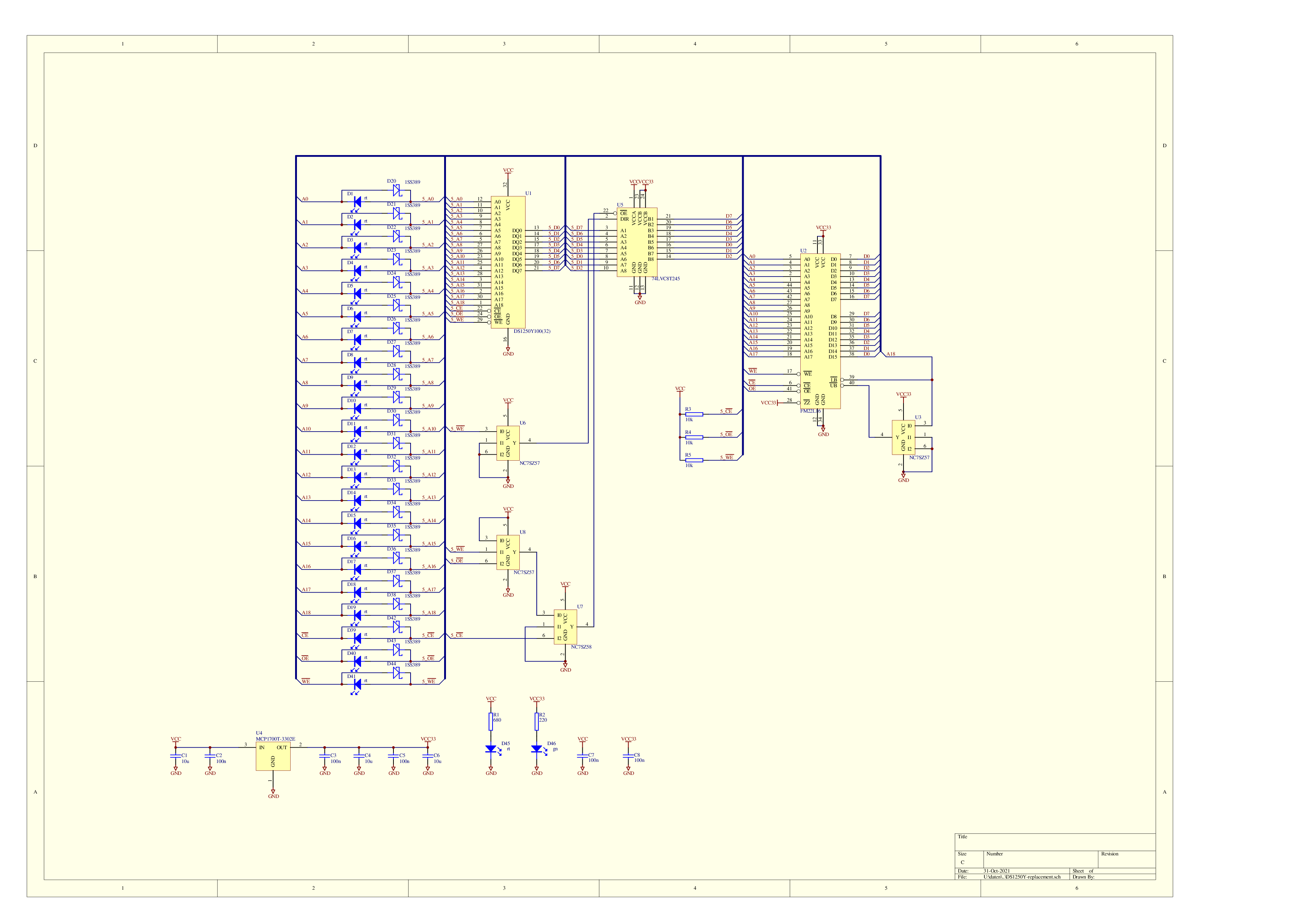
I used a bidirectional level shifter 74LVC8T245 for the data bus, a MCP1700T-3302E low dropout voltage regulator for the 3.3V power supply, a couple of universal single gates for the control logic and Schottky diodes and LEDs for the unidirectional level shifters of the address and control lines.

In the first version I had forgotten the pull-up resistors R3 to R5 which caused the data to be changed when the device was removed from the programmer. Otherwise, the circuit works flawlessly and easily meets the timing requirements of the original.

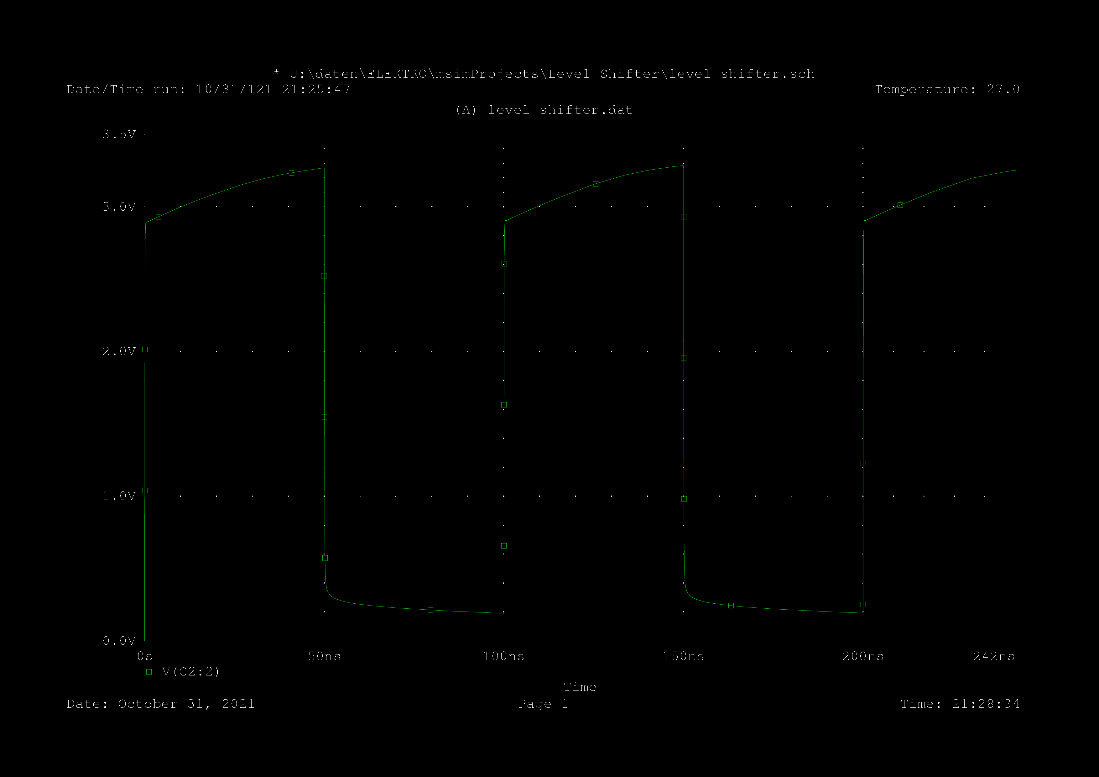
The unidirectional level shifters with a Schottky diode plus LED are still special and grown on my crap. I simulated the circuit and found that this simple way works safely and quickly.

Illustration, simulation of unidirectional level shifter
Simulation level shifter for address and control lines

The plan is available as a pdf here.
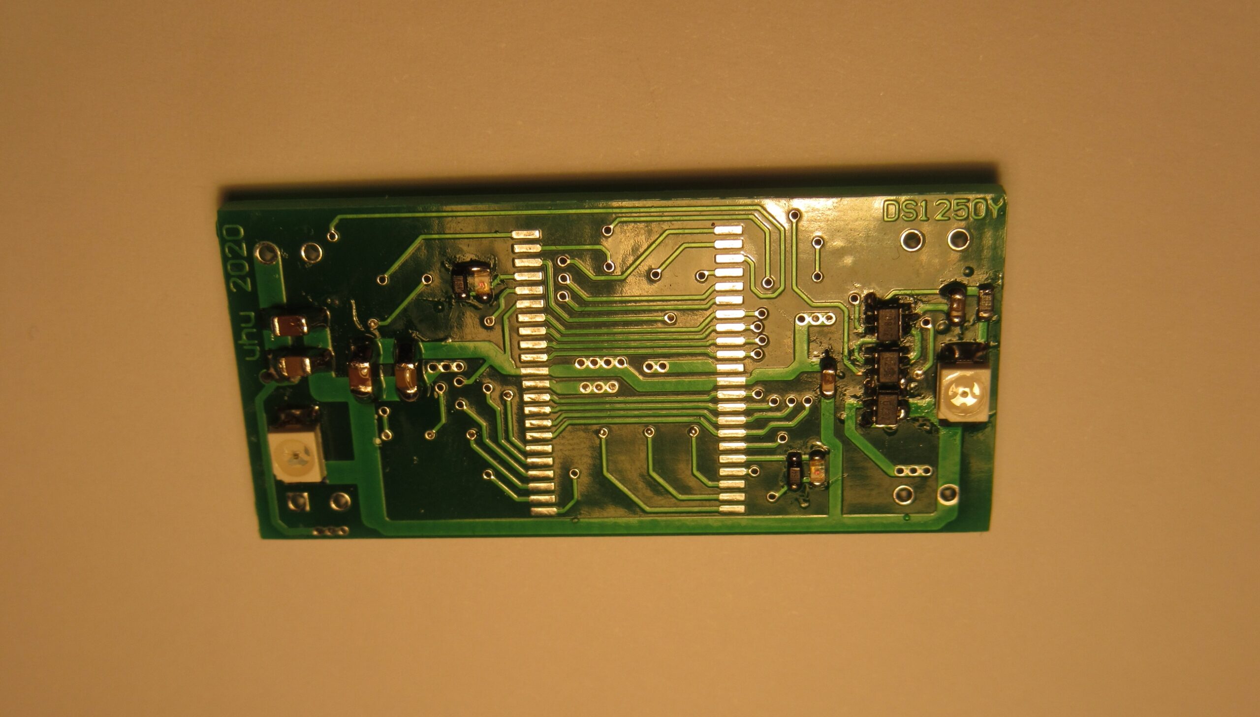
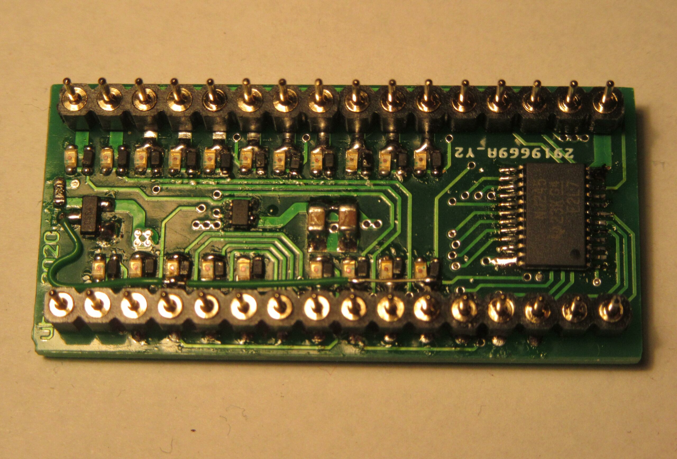
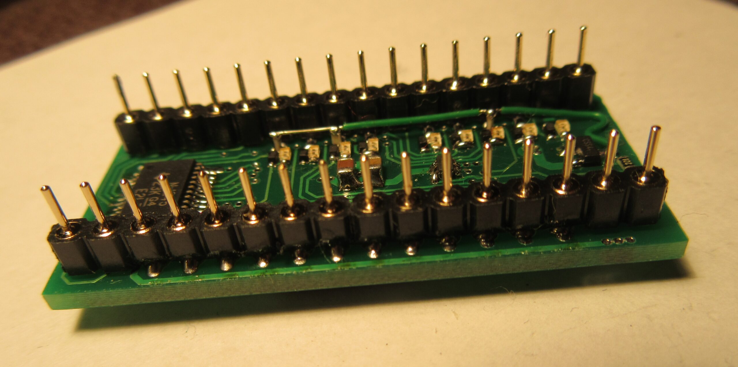
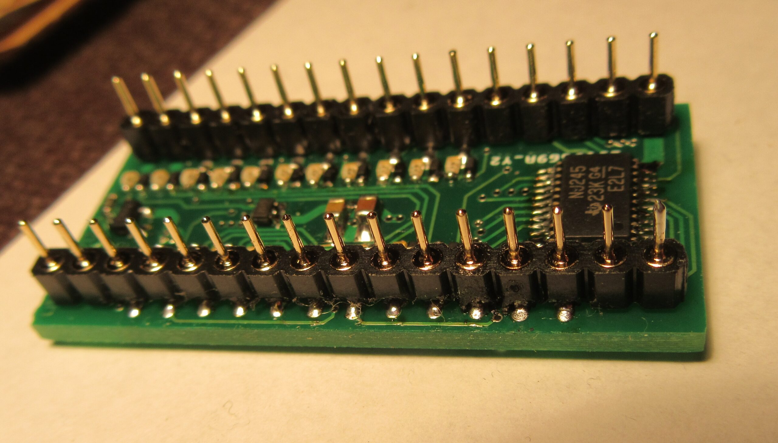
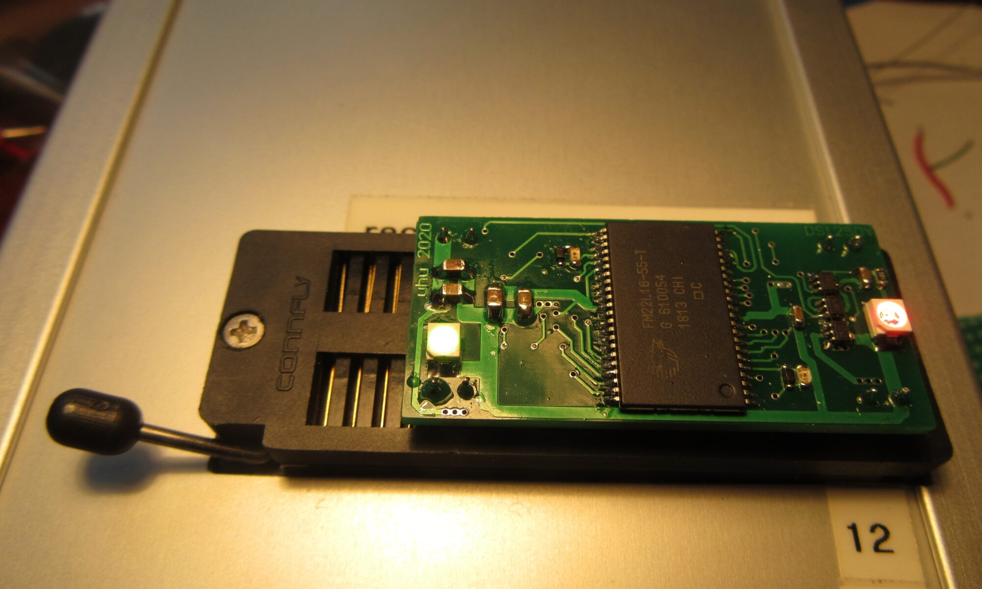
Contruction

The circuit is placed on a double-sided PCB, which is about 1mm wider than the original component. In most devices, however, there is enough space for it.

Abbildung, Layout
Board layout

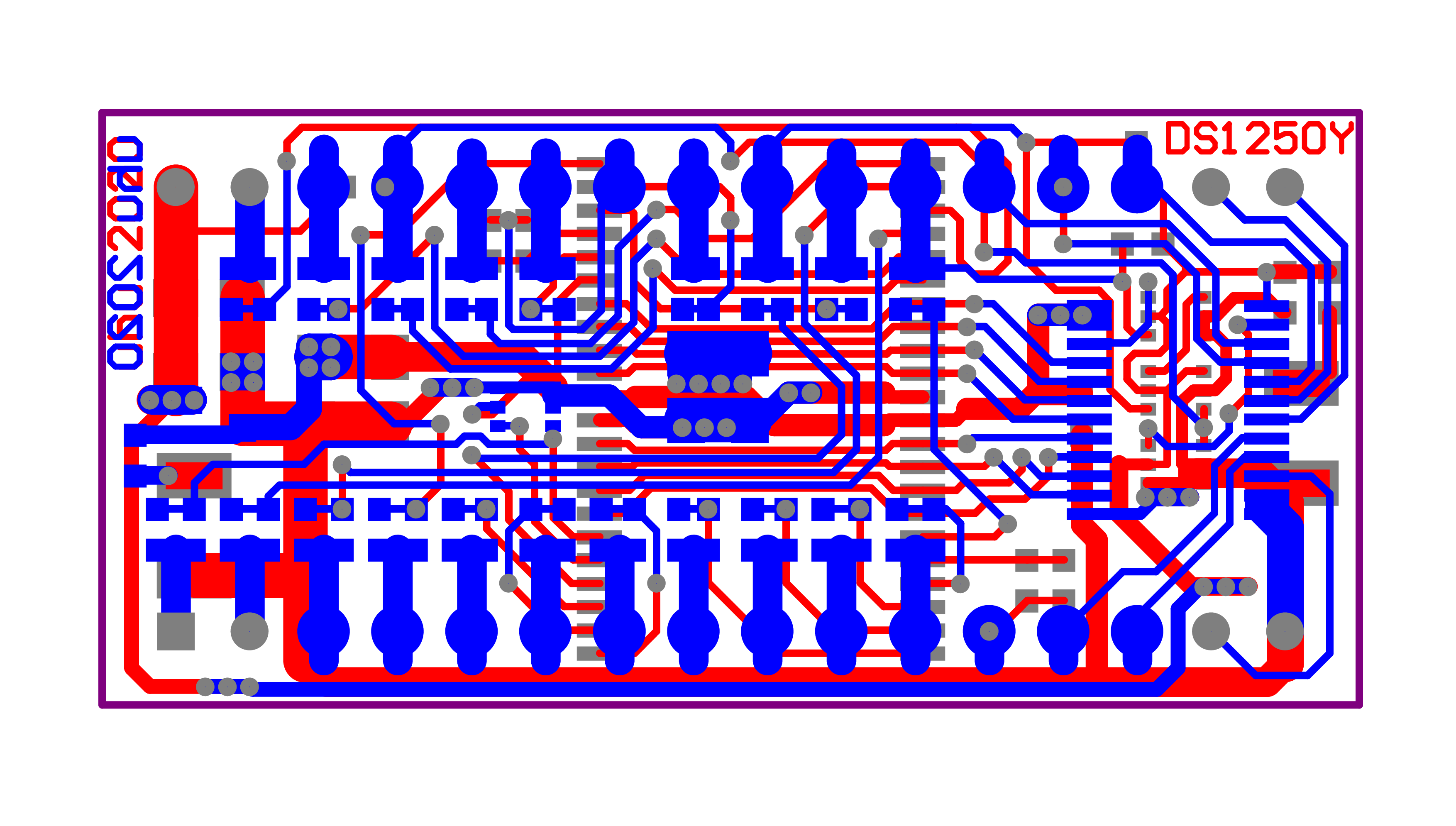
Gerber Files for private reorder are located here. Usually I order at JLCPCB. There you can simply upload the zip for ordering. The bill of materials and the assembly plan are here.

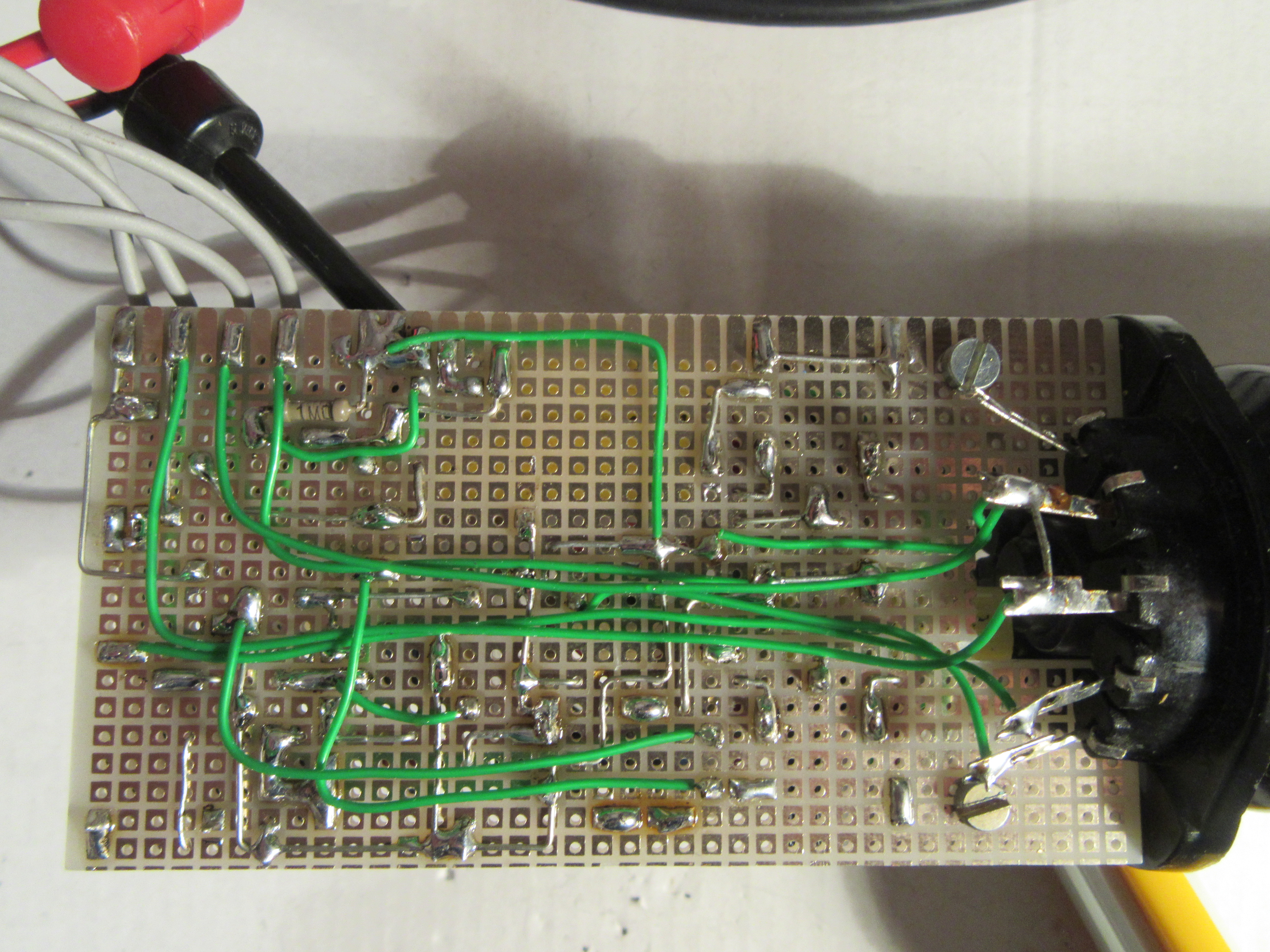
The rest follows as a short picture story:

Figure, finished boards are there and are assembled
Finished boards are there and are assembled
Figure, components manually assembled and soldered
Components manually assembled and soldered
Figure, bottom view
Bottom view
Figure, bottom view, afterwards added pull ups connected with wire, modification added to published design
Bottom view, afterwards added pull ups connected with wire, modification added to published design
Figure, bottom view, pin header manually soldered from beside
Bottom view, pin header fiddly soldered from beside
Figure, first prototype in the programmer
First prototype in the programmer


Receive updates directly in your inbox

Loading

Test oscilloscope tube Telefunken O7S1

First, I have to give a quick heads up: this post is a little longer than usual but that’s how it is with a hobby. You have a plan, you learn new things in the middle of it, and you expand a project piece by piece. A hobby is not about efficiency, but about making something “beautiful” and being satisfied at the end. So it doesn’t take long to add a few extra weekends of tinkering to something that should only take a few hours…
From the planned test of the O7S1 had resulted in the course of the time also these points:

  • Sawtooth generator, test setup and simulation with PSpice
  • Amplifier for X- and Y-deflection with double triode 6N2P
  • Overall circuit for a mini oscilloscope

But now let’s get started with the article.


Recently I rebuilt an old oscilloscope “Picoscope”. Among some other things the cathode ray tube was missing. In the original device a B7S1 from VEB Funkwerk Erfurt (part of RFT) is installed. The designators of such tubes are usually composed like in this case: A letter followed by the screen diagonal and the more exact designation. In this case, B7S1 probably stands for picture tube, 7cm diagonal, system 1. After a short internet search for this spare part, I didn’t find a B7S1, but an O7S1 for a relatively low price. A further search in my tube codex from 1948

Röhren-Codex 1948
“Röhren-Codex” 1948

and at radiomuseum.org revealed that an O7S1 is a pre-1945 Telefunken picture tube model. It has the same heater voltage and apparently the same socket circuitry as a B7S1. Further data on the O7S1 was not available. Unfortunately, my “Röhren-Taschenbuch” from 1958 from the “Fachbuchverlag Leipzig” does not contain the B7S1 yet.

Röhren-Taschenbuch Band II, 1958
“Röhren-Taschenbuch” Volume II, 1958

However, the similarity between the two tubes led me to believe that the B7S1 from RFT from the 50s is a compatible replica of the Telefunken tube from the 40s. So I bought it without further ado and after a few days the tube arrived undamaged. The first sight was good. Externally and mechanically everything was apparently in order, the contacts had not been in a socket for ages. This can be seen quite easily with a magnifying glass on corroded but not scratched contacts. Also the Telefunken logo and the designation are still held diagonally against the light, quite good to see. The silver inscription O7S1 is applied from modern times with one of these special pens.

O7S1 Bezeichnung und Telefunken Logo
O7S1 designation and Telefunken logo

On the base itself was the original imprint V II / RÖ 19. It occurred to me briefly whether it might not be Roman seven, but V Roman two or V2. Probably, however, it means assembly 7 / tube 19. If anyone knows which device it could be, I absolutely ask for a message.

O7S1 Sockel Detail
O7S1 socket detail

Since I still have an original Picoscope EO1/7, I could put the tube in there and do a quick test. But everything remained dark. Nevertheless, I did not give the online dealer a bad rating at first, but set up a test circuit. Very helpful was the page of Burkhard Kainka, on which beside many basics as well as small and large tinkering projects also a test circuit for a mini-oscilloscope is published. At this point a big thank you from me to the operator of the site for the work to publish all this.


Back to the test circuit: During the setup it quickly became clear that the sockets of the two tubes B7S1 and O7S1 are rotated by 180° and after a short time I could see that the tube basically works.

O7S1 Erster Test
O7S1 First test

What followed was a few weekends of tinkering. First I found out that grid 1 has no function anymore. This means that direct brightness control is no longer possible. This is not so much a problem, because you can also regulate the brightness with the anode voltage. However, it may also affect the focus, and probably the tube will no longer have the performance it had in its original state. Nevertheless I tried to develop the best possible circuit. Basis was as described above the test circuit of Burkhard Kainka.

First I tried to improve the X-deflection. Ideal is a sawtooth generator, which has a linear voltage rise and very fast fall. However, the original flip-flop circuit with a glow lamp gives an exponential voltage waveform. You can see this very clearly in the oscillogram in the article by Burkhard Kainka, the curve is compressed on the right. My idea should be as simple but a bit better and finally I experimented with a sawtooth generator with a unijunction transistor (UJT), whose basic circuit is quite simple.

Schaltbild PSpice Simulation Sägezahngenerator mit UJT 2N2646 erster Versuch
Schematic PSpice simulation sawtooth generator with UJT 2N2646 first try

At the emitter a sawtooth can be taken, which is already a bit more linear than a toggle circuit with glow lamps. Of course it is again the charge curve of a capacitor or an e-function. But here we are only in the lower range. A simulation with PSpice shows the expected, a not quite linear increase.

PSpice Simulation Sägezahngenerator mit UJT 2N2646, erster Versuch
PSpice simulation sawtooth generator with UJT 2N2646, first try

Since the frequency should be variable, I have inserted a resistor into the circuit, which is changed during the simulation via a parameter. With PSpice this is done by placing a global parameter on the worksheet, in this case V_POT. Several simulations are then run and this parameter is changed. I have chosen steps of 0.2 between zero and one. Via C2 and R4 the load of the generator is represented.

Schaltbild PSpice Simulation Sägezahngenerator mit UJT 2N2646
Schematic PSpice Simulation Sawtooth Generator with UJT 2N2646

Again, the simulation did not reveal any surprises. However, it was quite difficult to get the convergence problems under control with PSpice. This is especially problematic when simulating oscillators and one has to experiment with some simulation parameters until everything runs error-free to the end.

The frequency is adjustable within wide limits, we now have an excellent sawtooth generator for the X-deflection.

PSpice Simulation Sägezahngenerator mit UJT 2N2646, 7.5ms
PSpice simulation sawtooth generator with UJT 2N2646, 7.5ms

And another clip of the first half millisecond.

PSpice Simulation Sägezahngenerator mit UJT 2N2646, 500µs
PSpice simulation sawtooth generator with UJT 2N2646, 500µs

At the end I made an oscillogram of the built up sawtooth generator at minimum frequency, so it should look like the green curve. And voila it looks pretty similar. The amplitude is a bit higher and the frequency is a bit lower. I blame this on the component tolerances.

Oszillogramm Sägezahngenerator mit UJT 2N2646
Oscillogram sawtooth generator with UJT 2N2646

The sensitivity of the O7S1 is rather moderate. The exact value is not known to me. My tests showed about 50V/cm for the X- and 40V/cm for the Y-deflection. This left the next task to be solved, to amplify the signal by a factor of 25 to 30. True to style I chose a triode. The high voltage for the picture tube is available anyway, so the use of another tube does not mean a big additional effort. As a triode with high amplification an ECC83 is a good choice. Because of the high price of the ECC83 I chose the very similar 6N2P or 6H2П, which is still manufactured in Russia. As circuit a standard amplifier circuit for triodes is used. Here is the section of the overall circuit diagram of the mini-oscilloscope.

Schaltbild Verstärker mit Triode
Circuit diagram amplifier with triode

The second system of the double triode was used for the Y-amplifier, which is constructed identically to the X-amplifier. Some of the deflection plates must have a higher potential than the anode to be able to shift the X and Y origin over the whole visible range. This function is realized by some voltage dividers and potentiometers (R9 to R19 and P2/P3). With potentiometer P4 the focus is set. With this the mini-oscilloscope worked reasonably well and I was satisfied.

Finally the complete schematic, a photo gallery and a short video.

Vollständiges Schaltbild
Complete schematic


Mini-Oszilloskop komplett
Mini oscilloscope complete


Mini-Oszilloskop Elektronik
Mini Oscilloscope Electronics


Sawtooth generator with unijunction transistor 2N2646


Mini-Oszilloskop Elektronik von unten
Mini oscilloscope electronics from below

Sine, square and triangle signals approx. 2kHz from my function generator.

Sinus Rechteck Dreieck

The tubes glow.

This is what the whole thing looks like live, fed from the function generator.


Receive updates directly in your inbox

Loading